

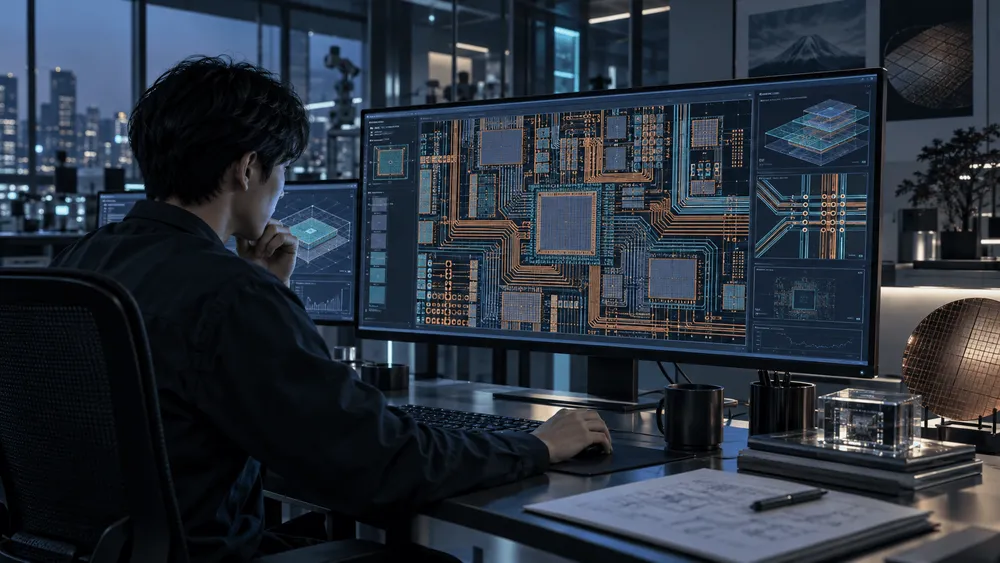
Chinese EDA company Empyrean Technology (华大九天) used an AI agent to cut the time needed for a circuit layout task from four weeks to one week, South China Morning Post (SCMP) reported on September 13, 2026. The example was cited by company chairman Liu Weiping, and it points to a shift in how software for designing and verifying circuits is being used. The company is also working on multilayer circuit designs that align with the "Tau Law" concept promoted by Huawei. Whether Empyrean can speed up designers' work while still correctly verifying increasingly complex circuits will be the real measure of its progress.
From Four Weeks to One: The Scope of the Speedup
According to SCMP, Empyrean applied AI agents to its simulation and layout tools, shortening the time required for a specific circuit layout task. Speaking at the International Semiconductor Innovation Expo in Shenzhen, Liu described a shift away from engineers directly operating tools toward engineers issuing instructions to agents instead.
EDA stands for electronic design automation, referring to the suite of software that supports circuit design, physical layout, and verification. Because layout involves deciding where to place circuit elements and how to route wiring, it is closely tied to the simulation process used to check circuit behavior. Embedding AI into this workflow creates room to reduce the repetitive operations designers have long performed.
However, the "four weeks to one week" figure refers to the outcome of a single task cited by the chairman. The publicly available portion of the SCMP report does not specify the scale of the circuit involved, the computing resources used, or whether the same quality was maintained for comparison. It is also unclear whether the timeframe includes revisions and final verification, so the figure cannot be directly applied to the overall time or cost of chip development.
Still, the description of agents calling on existing tools carries real significance for product development. Scaling automation requires that tools respond to agent instructions and that results can be passed on to the next stage of design work. Alongside this shift in how tools are used, Empyrean also faces the challenge of handling increasingly complex circuits themselves.
How Tau Law Is Reshaping Circuit and Wiring Design
On May 25, 2026, Huawei unveiled Tau Law as a guiding concept for the evolution of semiconductors. Whereas conventional miniaturization focuses on shrinking the geometric dimensions of components, Huawei's proposal centers on reducing the time it takes for signals to propagate, such as delay. The concept extends from individual components to circuits, and further to chips and systems, with the aim of optimizing each level in coordination with the others.
The technology responsible for this at the circuit level is called LogicFolding. Huawei explains that by rearranging circuit layouts, wiring along critical paths can be shortened, reducing the resistance and capacitance loads that affect signal propagation. What this aims to reduce is a different kind of time than the number of days designers spend on a task—it is the delay experienced by signals as they travel through wiring, with the goal of improving circuit performance.
Handling layouts that span multiple layers requires EDA tools themselves to evolve. In a September 1 interview with China Securities Journal, Liu explained that system-level design planning and 3D physical implementation present challenges. He added that verification and reliability analysis spanning multiple semiconductor dies—the individual pieces cut from a wafer—are also required. Compared with designs completed within a single layer, this requires confirming operation while accounting for connections to other layers as well.
According to Liu, Empyrean has unified foundational data across its product lines and rebuilt its software architecture accordingly. He said a solution that integrates 3D design and verification has already been applied by customers and has supported tape-out, the process of handing off design data for manufacturing. However, this description refers to the company's broader efforts and has not been confirmed to be the same project as the AI-driven time reduction discussed above.
The changes that AI and Tau Law are demanding of EDA can be broken down as follows:
| What Is Being Assessed | Change or Goal Demonstrated | What Still Needs Confirmation |
|---|---|---|
| AI-driven circuit layout work | Chairman's account describes a reduction from four weeks to one week | The circuit involved, computing resources used, quality maintained, and whether the timeframe includes revisions |
| Circuit design aligned with Tau Law | Huawei states that it reduces signal delay through wiring and related factors | Capability to implement and verify designs across multiple layers |
| Final pre-manufacturing verification | Liu anticipates that analysis tools and human judgment will remain necessary | Whether compatibility between design and manufacturing processes can still be confirmed after automation |
Faster completion of a task and faster performance of the finished circuit are two separate achievements, each requiring its own evaluation. The business opportunity for EDA tools aligned with Tau Law likely lies in the new demand for designing and verifying such circuits. The reported time reduction alone cannot be used to draw conclusions about circuit performance or advantages over competing tools.
Tasks Left to AI, and Tasks Left to Human Judgment
Liu himself does not view AI agents as capable of replacing all of EDA. In his interview with China Securities Journal, he suggested that while design, implementation, and iterative optimization are moving toward an agent-based model, simulation and verification involving scientific computation will continue to rely on conventional tools. He also stated that human judgment will remain necessary for sign-off—the final verification and approval stage before manufacturing begins.
Under this framework, the capability of AI agents and the reliability of the analysis tools they call upon need to be evaluated together. Even if AI can rapidly iterate on layout changes, the role of confirming that the finished design works correctly and is compatible with the manufacturing process still remains. If the time required for revisions leading up to verification can also be shortened, it will become easier for design teams to judge the actual value of these results.
Practical deployment also brings burdens related to data and computing resources. Liu pointed to the fragmentation between high-quality design data used for training and manufacturing process data as a challenge, noting that cooperation from foundries—companies that manufacture semiconductors on contract—will be necessary. He also acknowledged that both developing and using agent-based EDA tools will require substantial computing resources.
Pricing structures may also change. Liu outlined a future business model combining traditional software licenses with token-based agent services. This remains a vision for the future, not an announcement that Empyrean has already introduced new pricing. When considering costs, users will need to weigh not only task completion time but also the computing resources required.
The next test for Empyrean will be whether it can clearly disclose the circuits involved and the verification conditions used, and demonstrate that it can shorten development—including the time from revisions through sign-off. If such results can be replicated consistently, even for multilayer circuit designs, designers would be able to spend less time on repetitive operations and devote more effort to refining circuit architecture and handling complex judgment calls.