


The jet-black panels of satellites orbiting at an altitude of 400 kilometers are fundamentally different from the solar cells we see on the ground. To wring out every last drop of power from a limited surface area, they employ a multi-junction structure that stacks three or four dedicated semiconductor layers, each tuned to a different wavelength of light. Manufacturing these space-grade panels requires advanced vacuum processes and rare elements, driving the cost per watt to roughly 1,000 times that of terrestrial silicon panels. Lining the roofs of the houses we live in with such panels has long been considered economically impossible.
Three layers of sieves scooping up the full spectrum of sunlight
Currently, crystalline silicon solar cells account for over 90% of the global photovoltaic market. While the maturation of manufacturing technology has driven dramatic cost reductions, the limits of photoelectric conversion using a single material are now in plain sight. No single semiconductor material can convert the full breadth of energies present in sunlight into electricity. The Shockley–Queisser limit, which defines the physical upper bound on conversion efficiency, sits at around 29%, and even the top-tier products on the market today have already plateaued near 22–24%.
The approach for breaking through this ceiling is multi-junction technology, which stacks multiple different materials together. A triple-junction structure can be likened to three sieves with different mesh sizes stacked on top of one another. The top cell at the very top has the coarsest mesh, capturing only high-energy blue photons. The middle cell has a slightly finer mesh, scooping up the intermediate green and yellow light. And the bottom cell, with the finest mesh of all, catches the low-energy infrared light that slips through the two layers above without missing a beam. When each layer handles only the wavelength band it is best suited to absorb, energy that would otherwise escape as heat can be recovered to the fullest extent, theoretically making efficiencies exceeding 50% attainable.
How perovskite upended the silicon-dominant premise
Until now, realizing this multi-junction structure required expensive III-V semiconductors made from materials like gallium and arsenic—an approach confined to space applications where budgets in the millions of dollars were permissible.
But in recent years, perovskite semiconductors have emerged that can be manufactured through inexpensive solution-coating processes and whose bandgap—the property that determines which wavelengths of light they absorb—can be freely tuned simply by altering their chemical composition. With the advent of techniques for coating perovskite directly onto silicon, or stacking multiple perovskite layers on top of one another, a path has opened up to achieve space-grade performance at ground-level cost. The question now is how best to integrate this new family of materials into precisely engineered multi-junction devices.
A silicon-perovskite trio reaches 30.02% through optical design
A joint research team from the PV-Lab at the Swiss Federal Institute of Technology Lausanne (EPFL) and the Swiss Center for Electronics and Microtechnology (CSEM) has refined this multi-junction approach to an extreme degree. They built a 1 triple-junction solar cell by placing a conventional silicon solar cell as the base layer and stacking two perovskite thin films with different properties on top of it, achieving a power conversion efficiency of 30.02% as certified by an independent institution.
This marks a substantial improvement—nearly 3 percentage points—over the previous record of 27.10% held by a research team at the National University of Singapore. Having completely left the theoretical limit of single-junction silicon in the dust, this record signals that perovskite technology has entered a transitional phase, moving from lab-scale prototypes toward practical, ultra-high-efficiency devices.
Managing light and electrons through nanoparticles and crystal control
The biggest obstacles facing the EPFL and CSEM team were two bottlenecks: low voltage in the top cell and low current in the middle cell. In a triple-junction solar cell connected in series, the layer that generates the least current drags down the performance of the entire stack. The team resolved this physical constraint through three precise technical interventions.
First, when forming the perovskite layer of the top cell, they introduced a special molecule that guides crystal growth and seals microscopic surface defects. This suppressed the phenomenon in which electrons generated by absorbed light become trapped in defects and vanish before reaching the electrode, allowing them to achieve an extremely high open-circuit voltage of 1.4 V in the top cell alone.
Second, they introduced a new solution process for manufacturing the middle cell, dramatically improving the absorption efficiency in the near-infrared band that had previously been missed.
The third innovation is the most important. They incorporated a regular arrangement of silicon oxide () nanoparticles between the middle cell and the bottom silicon cell. This nanoparticle layer acts as a microscopic mirror that selectively reflects light of specific wavelengths. By forcibly reflecting intermediate-wavelength light—which had previously been leaking excessively through to the bottom silicon layer—back up into the middle cell, they physically boosted the current generated within the middle cell, bringing the current balance across all three layers into perfect alignment.
The interfacial noise plaguing the all-perovskite alternative
While EPFL used silicon as a solid foundation, a research team at the Helmholtz-Zentrum Berlin (HZB) in Germany is pursuing a different approach to push past the limit: an all-perovskite triple junction that uses no silicon at all, constructing all three layers entirely from perovskite. In its latest research, HZB achieved an efficiency of 27.3% while simultaneously and dramatically boosting the durability that has been the Achilles' heel of this type of device.
The biggest weak point in a fully perovskite structure is the tin-lead (Sn-Pb) mixed perovskite layer positioned at the bottom. Until now, a conductive polymer called PEDOT:PSS has been the standard material used to extract positively charged holes from this layer. This polymer is acidic and highly hygroscopic, readily oxidizing the tin and destroying the device from within. On top of that, the polymer itself causes a phenomenon known as parasitic absorption, wastefully absorbing light and making current losses unavoidable.
As an alternative, researchers have attempted to use self-assembled monolayers (SAMs), which have proven successful in lead-based solar cells. A SAM is a molecular film only a few nanometers thick that absorbs almost no light, but for some reason, when placed directly beneath a tin-lead perovskite layer, charge extraction deteriorated drastically, causing efficiency to drop.
The HZB research team conducted in-depth analysis, including transient surface photovoltage (trSPV) measurements, and identified the cause. With the SAM molecular layer alone, iodine ions and other species within the perovskite migrated to the interface and shielded the internal electric field, hindering the smooth separation of electrons and holes.
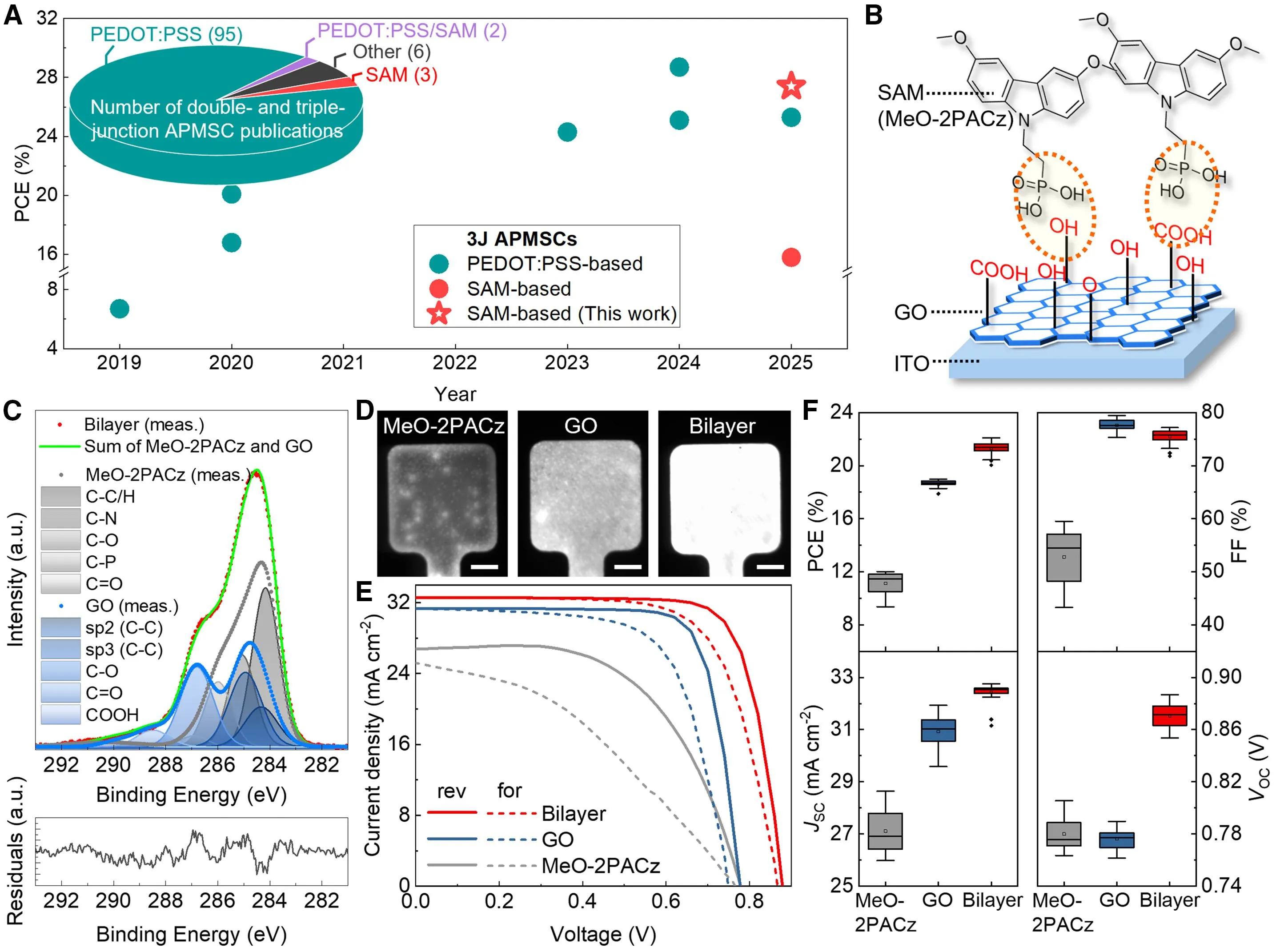
Graphene oxide as fertile soil, and 770 hours of stability
The solution HZB arrived at was to lay an ultra-thin layer of graphene oxide (GO) beneath the SAM molecules, forming a bilayer.
This mechanism resembles sowing seeds in agriculture. If the SAM molecules are the seeds of a plant, GO plays the role of fertile soil. Scattering SAM molecules directly onto the surface of an inorganic electrode does not allow them to take root uniformly, but by first laying down GO, which is rich in oxygen functional groups, the SAM molecules bond chemically with the GO and align themselves in a regular, robust fashion. The result is a densely packed forest through which charge can flow without getting lost.
With the introduction of this GO/SAM bilayer, the short-circuit current density of a single-junction tin-lead perovskite cell improved by 5.8 compared to using SAM alone, achieving a conversion efficiency of 22.1%. The team applied this technology to a triple-junction device, completely eliminating the parasitic absorption caused by PEDOT:PSS. By precisely tuning the bandgaps of the middle and bottom cells, they reached an overall device efficiency of 27.3% across all three layers.
Even more significant is the extended lifespan achieved by suppressing the noise from oxidation and ion migration. In continuous light-soaking tests, the triple-junction device equipped with the GO/SAM bilayer maintained over 90% of its initial efficiency even after 770 hours had elapsed. Compared to the conventional structure using PEDOT:PSS, which reached its degradation threshold at around 380 hours, this represents a doubling of stability—a world-leading durability record for all-perovskite triple junctions.
| Approach | Developing Institution | Cell Configuration (Top / Middle / Bottom) | Conversion Efficiency | Key Technical Breakthrough | Challenges and Remaining Hurdles |
|---|---|---|---|---|---|
| Perovskite/silicon hybrid | EPFL & CSEM | Perovskite / Perovskite / Silicon | 30.02% | Light reflection via nanoparticles, voltage improvement via crystal-control molecules | Manufacturing cost due to the presence of the silicon layer, long-term durability outdoors |
| Fully perovskite | HZB | Perovskite / Perovskite / Sn-Pb perovskite | 27.3% | Elimination of parasitic absorption and suppression of ion migration via GO/SAM bilayer | Preventing tin oxidation, uniformity of film formation in large-area module fabrication |
| (Reference) Space-grade compound cells | Various aerospace companies | III-V semiconductors (GaInP / GaAs / Ge, etc.) | ~37% | Ultimate efficiency via perfect lattice matching and epitaxial growth | Manufacturing cost impractical for consumer use (roughly 1,000x that of silicon-based cells) |
Scaling up and sealing hurdles on the road to space technology on your rooftop
EPFL's 30.02% milestone is not merely a theoretical exercise—it proves, at the actual device level, that this approach has completely surpassed existing single-junction silicon. At the same time, HZB's achievement of 27.3% and long-term stability with an all-perovskite structure is making the future of lightweight, flexible, ultra-high-efficiency panels—which would eliminate even the need for a thick, rigid silicon wafer substrate—a realistic prospect.
To bring this physical breakthrough, demonstrated in small 1 lab devices, into implementation as social infrastructure, the next steps are needed. The greatest challenge is establishing a mass-production process capable of continuously coating nanometer-scale thin films without defects, uniformly, across large-area glass substrates or plastic films. When transitioning to industrial roll-to-roll methods or slit-die coating processes, the slight drying unevenness or thickness variations that never surfaced in small-scale laboratory spin-coating can become factors that significantly degrade the performance of an entire module.
Another unresolved question is how to guarantee the more than 20 years of outdoor durability required of solar modules. Because perovskite materials are inherently extremely vulnerable to moisture and oxygen, developing rigorous packaging technology using special resins such as ethylene vinyl acetate (EVA) or polyolefin elastomer (POE) is becoming just as important as—if not more important than—improving the materials themselves.
An extravagant, ultra-high-efficiency technology once permitted only in the vacuum of space is now borrowing the familiar manufacturing method of printing processes. The countdown has already begun toward the day when it blankets every rooftop and wall surface on the ground.