

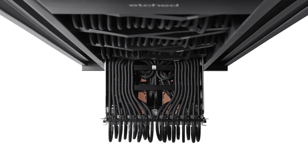
Etched shipped its first inference rack to Jane Street in July 2026, and the company's data center began running it. On August 18, the company also announced a $700 million funding round and a $21 billion valuation. Back in late June, the company had touted a "working chip" and plans for its first shipment that summer; the substantive change now is that it has moved to the stage of running racks in a customer's own facility.
Jane Street is both the lead investor in this round and the first customer Etched has publicly named. The fact that a customer is running the rack inside its own data center serves as evidence distinct from design success or A0 silicon success. That said, what's been disclosed is just the first single rack for one specific customer. The workloads being processed, the number of units, utilization rates, SLAs, and pricing all remain undisclosed. A $21 billion valuation does not equate to revenue or independently verified performance.
Valuation roughly doubles in 26 days, but the terms don't line up
Etched announced a $300 million Series C and a $10.3 billion valuation on July 23. Sequoia described this round as having a $10 billion pre-money valuation, which is consistent with a $10.3 billion post-money figure after adding the $300 million. By contrast, the August 18 announcement cited $700 million raised and a $21 billion valuation, but did not specify a round name or whether the figure was pre-money or post-money.
| Date | Funding / Valuation | Product / Deployment Stage |
|---|---|---|
| June 30, 2026 | $800 million raised cumulatively; post-money valuation of $5 billion at the time of the $500 million raise in December 2025 | A0 silicon on TSMC N4P, customer validation, first rack shipment planned for summer |
| July 23, 2026 | $300 million Series C, $10.3 billion valuation | Announced initial manufacturing and expansion of customer deployments |
| August 18, 2026 | $700 million led by Jane Street, $21 billion valuation | First single rack shipped to Jane Street in July, now running in the company's own data center |
The period from $10.3 billion to $21 billion spans just 26 days, and comparing the announced figures shows roughly a doubling. But since one figure aligns with a post-money valuation while the other's pre-money/post-money status is undisclosed, it cannot be said with rigor that a valuation under the same definition exactly doubled. The $5 billion figure from December 2025 was a post-money valuation, so this distinction needs to be kept in mind when comparing it to the $21 billion figure as well.
Etched states its cumulative funding raised at $1.9 billion. However, simply adding the $300 million from July and the $700 million from this latest round to the $800 million cumulative figure as of June 30 yields $1.8 billion. There may be undisclosed portions or rounding in past fundraising, but the company has not explained the discrepancy. The cumulative figure should be taken as the company's latest public statement, separate from any figure reconstructed purely from the disclosed rounds.
Jane Street: Both Investor and First Customer
Jane Street commented that it has tested the chip and is satisfied with the initial results. The firm also stated that its own rack is running inside its data center. Etched's CEO has said that Jane Street will bring this cluster into its own production environment, but Jane Street's own statement amounts to an early assessment that it can achieve the accuracy needed to support demanding workloads. It is not an announcement demonstrating broad production operation or established mass-production quality.
The significance of this deployment lies in confirming that the system runs in a customer's facility, ahead of any published benchmark figures. Getting a rack running requires not just compute and interconnect but also cooling and software tailored to the customer's environment. However, Jane Street is also the lead investor in this round and had participated in the July Series C as well. Its assessment is the testimony of an early customer with capital and commercial ties to the company, not an unbiased third-party benchmark.
Etched states it has customer contracts worth over $1 billion with multiple frontier AI companies and cloud providers. This figure is not recognized revenue. Contract terms, cancellation conditions, shipment volumes, and revenue recognition timing have not been disclosed. It also cannot be translated into backlog or actual shipment scale. The single rack running at Jane Street is a more concrete step forward than the contract figures, but it is not a number that measures market-wide adoption.
LVI and CSM: Two Designs Realized in the Inference Rack
Etched has disclosed two pieces of inference-specific hardware: Low Voltage Inference (LVI) and Cluster Scale Memory (CSM). LVI is a design that runs compute blocks at less than half the voltage of typical AI chips. The company claims that for trillion-parameter-class sparse Mixture of Experts (MoE) models, it can sustain over 80% of peak FLOPs without thermal throttling.
LLM inference load varies between prefill, which processes input in bulk, and decode, which generates output one token at a time. Prefill is more sensitive to compute density, while decode is bound by memory bandwidth and transfer latency due to repeated KV cache reads. LVI targets throughput for the former, while CSM targets responsiveness for the latter.
These are Etched's own claims; the model conditions, precision, and comparison targets have not been disclosed. Rack power consumption and measured data have also not been made public. Even if compute can run at low voltage, rack-level performance and power efficiency are determined by everything from memory access to thermal management to software implementation. Public figures alone do not allow third parties to reproduce how much of an advantage exists for which use cases.
CSM is a design that uses a proprietary low-latency, high-bandwidth interconnect to create a shared memory pool combining HBM and SRAM across the entire scale-up domain. For inference on massive models, how each chip reaches the weights and intermediate data it needs matters just as much as raw compute throughput. Etched builds this into the rack-level design. The capacity, bandwidth, and latency of the HBM and SRAM have not been disclosed. The coherency scheme and where faults are isolated also remain undisclosed.
What Remains After Adopting N4P: Manufacturing and Deployment
Etched's A0 silicon reportedly achieved first-pass success on TSMC's N4P process. According to TSMC, N4P is a performance-enhanced variant of the N5 family that entered mass production in 2023. TSMC's stated targets of 11% better performance, 22% better power efficiency, and 6% better density compared to N5 are process-level goals, not indicators of Etched's actual product performance.
Given that N4P itself is already in mass production, the difficult work remaining for Etched lies less in making the process node work and more in repeatedly manufacturing racks and continuing to deploy them to customers. As of July, the company had opened an 80,000-square-foot, 10MW facility in Milpitas, California. The plan is to use it for a new product introduction (NPI) lab, an in-house SMT line, and expanded deployment capacity, while its San Jose headquarters also houses a 2MW data center.
These facilities provide a foundation for bringing yield, component supply, and inspection processes closer in-house. Whether cooling, software, and customer deployment can proceed smoothly, however, is something that must be verified separately from whether the chip itself works. Etched says it is developing three generations of hardware in parallel, but has not disclosed the specifications or timing for each generation. Its ability to advance subsequent generations while maintaining the quality of the generation that has begun shipping will also be tested in the wake of this first rack.
The Numbers Needed to Measure a $21 Billion Valuation
This announcement adds concrete evidence at the implementation level: a rack running in a customer's data center. Even so, there isn't yet enough material to translate the valuation into performance or business scale. Only once the company publishes how latency and power were measured under identical models, precision, and batch conditions—and makes pricing comparable—will it be possible to judge the practical difference that LVI and CSM actually make.
On the customer side, visibility is needed into how many units have shipped to customers beyond Jane Street, when, and over what length of operating time. On the contract side, another point to verify is when and how much of that over-$1-billion contract figure gets recognized as revenue. The fact that the first single rack is now running is a starting point; what comes next is whether the same conditions can be reproduced across multiple customers and racks—that is what will tie the $21 billion valuation to concrete operational numbers.