


At Hot Chips 2026, Intel disclosed the internal architecture of its data center GPU under development, "Crescent Island." The chip packs 32 Xe3P-based Xe cores and 256 XMX matrix engines into a 350W air-cooled PCIe card, with Intel-branded versions carrying 160GB of LPDDR5X. Partner designs, Intel says, can scale up to 480GB. The goal isn't to compete as an all-purpose GPU chasing peak performance, but rather to handle the prefill phase of inference on long inputs and large numbers of memory-hungry sessions within existing server environments.
However, there are no real-world measurements yet to back up Intel's stated "tokens per watt" claims. Memory bandwidth also remains undisclosed, leaving open the question of how the capacity and 350W design will translate into actual response speed and operational cost—something that can only be confirmed once the product ships.
Beyond 32 Xe Cores: What Changed in Xe3P
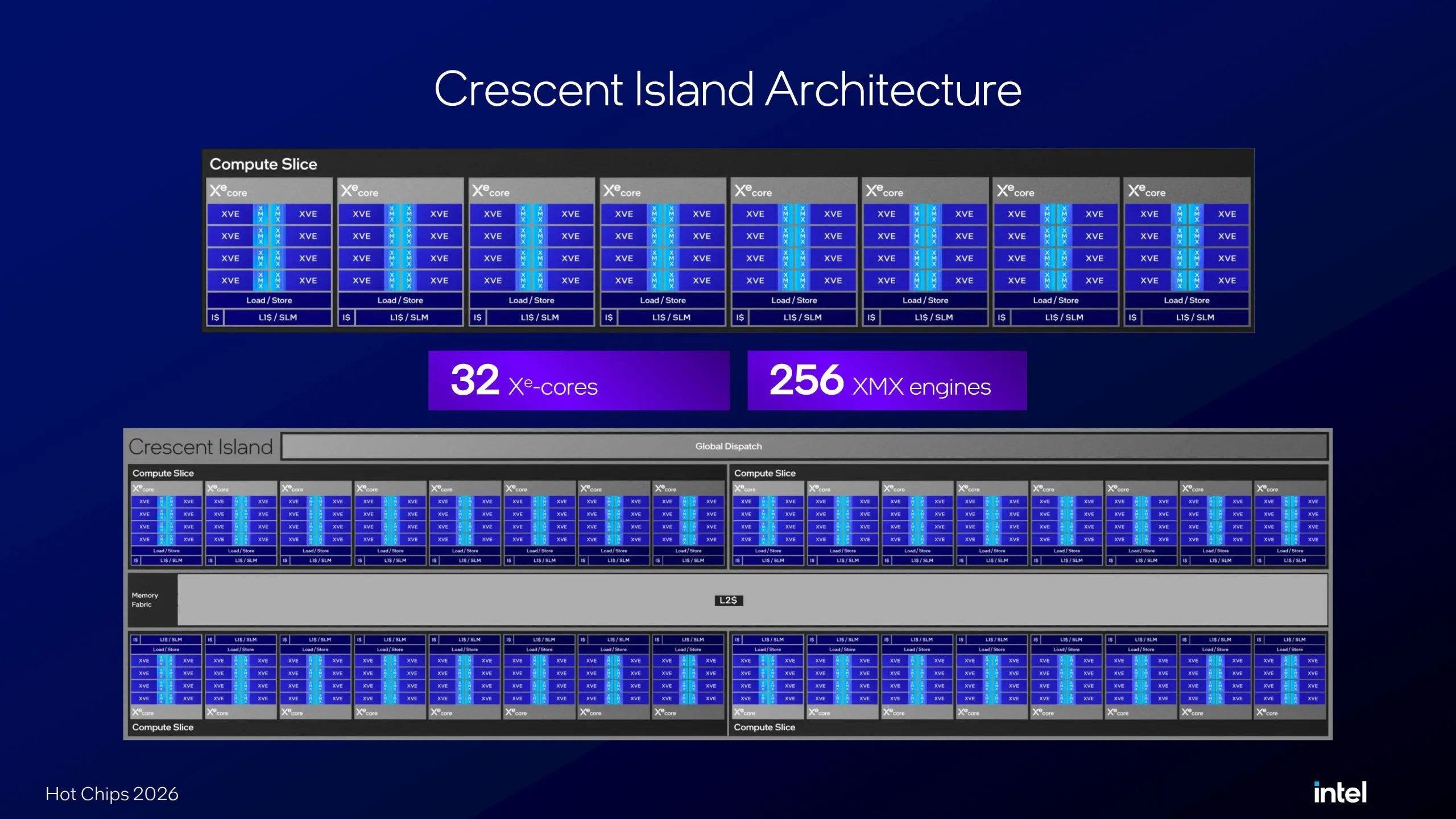
Crescent Island is built from four GPU slices, each containing 8 Xe cores. Each core has 8 Xe Vector Engines and 8 XMX Engines, totaling 256 of each across the whole GPU. The rework Intel places at the center of its inference performance story is the redesigned XMX.
While the XMX units in Xe2 and Xe3 used a 4-stage systolic array, Xe3P deepens this to 16 stages—a change that makes it easier to process matrices in larger chunks. That said, quadrupling the depth doesn't mean compute performance quadruples as well; actual effective performance can't be determined without knowing clock speeds, data supply, and utilization rates.
To keep data flowing continuously to the compute units, Intel also thickened the memory hierarchy. The general-purpose register file per Xe core doubled from 512KB to 1MB, and the L1 cache/shared local memory grew from Xe2's 256KB to 512KB. The shared L2 cache expanded from 18MB to 32MB—roughly 1.78x. These changes appear aimed at reducing how often working data that overflows registers must be evicted to distant memory, cutting down on XMX wait times.
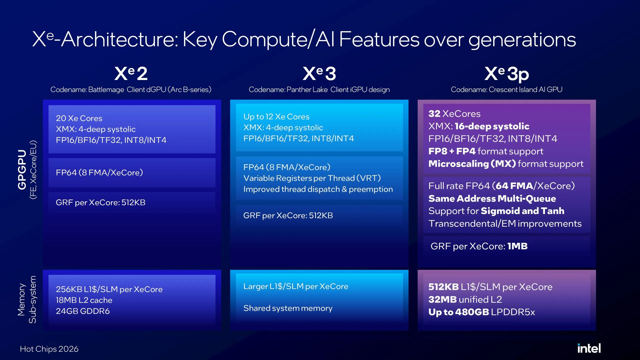
This configuration pairs well with the prefill phase of large language model inference. Prefill batches the input prompt through matrix operations to build the KV cache used in subsequent generation, while decode generates tokens sequentially and is therefore more sensitive to memory read speed. Intel itself describes Crescent Island as "prefill optimized," and has added FP4, FP8, and Microscaling formats. FP64 also gets full-rate support at 64 FMA per Xe core, preserving use cases that span both AI and HPC.
160GB Intel Cards, 480GB ODM Designs
The "up to 480GB" figure comes with a product boundary. According to a footnote on Intel's Hot Chips slide, Intel-branded PCIe cards carry 160GB, while 480GB is the upper limit for ODM cards designed by partners. An Intel-branded card with 480GB has not been finalized as a standard SKU.
Even so, 160GB is substantial for a single card. Fitting model weights and KV cache onto the same GPU more easily reduces the need for cross-GPU communication. Given the same model, the extra capacity can be redirected toward more concurrent sessions or longer contexts. The up-to-480GB design option extends that headroom to three times the Intel-branded product.
Capacity is not a substitute for bandwidth. Intel has not disclosed the LPDDR5X speed, bus width, or effective bandwidth, making it impossible to judge whether data can be supplied to the 256 XMX units fast enough. The name "LPDDR5X" alone doesn't guarantee it will always be cheaper or easier to procure than HBM. The cards connect via PCIe Gen5 x16, but whether a dedicated link exists for bundling multiple GPUs together also remains unclear.
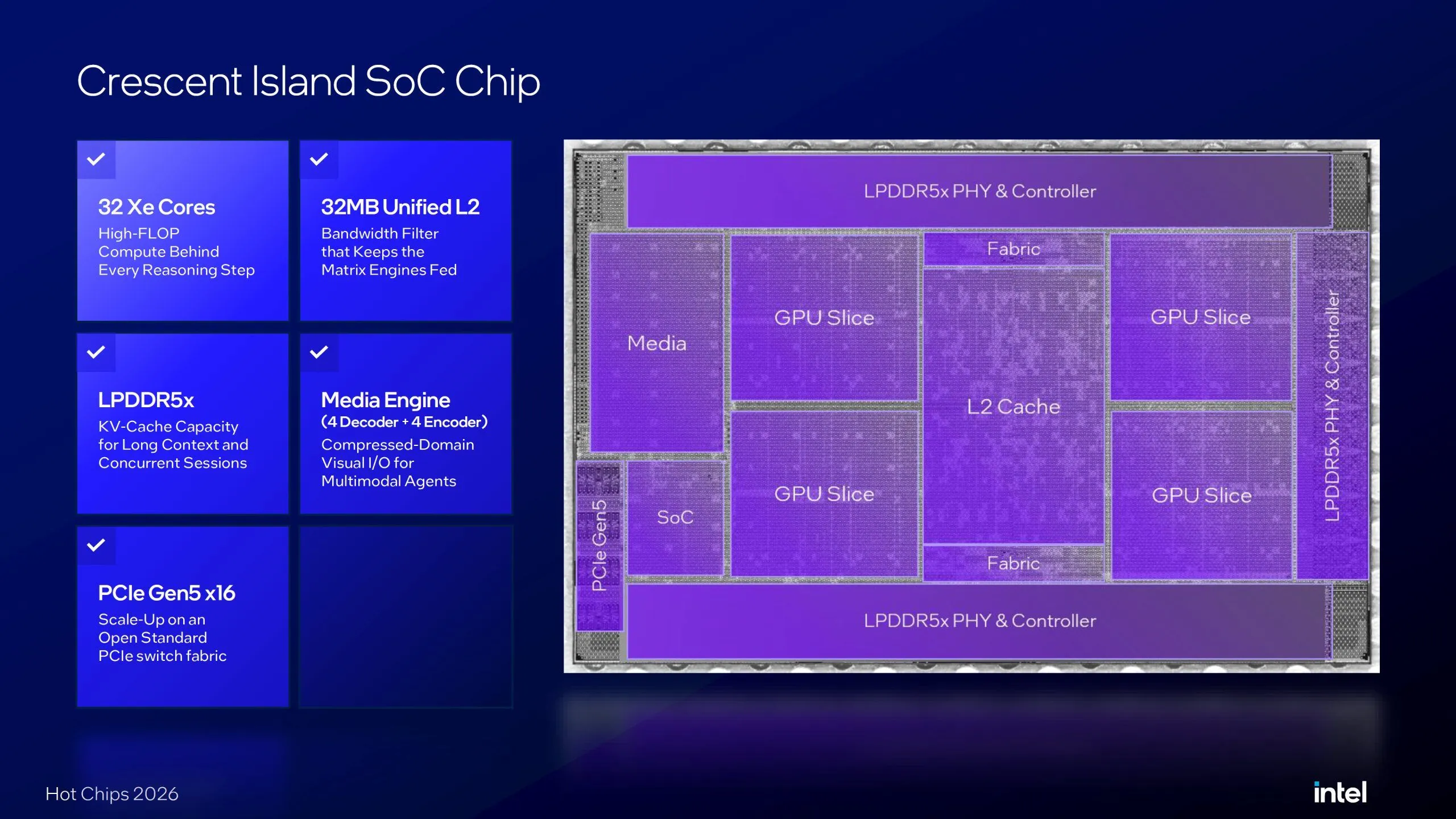
The SoC also includes a media engine with four video encoders and four decoders. For multimodal inference that handles video, this makes it easier to complete compressed-data processing within the GPU itself. In contrast, the disclosed architecture diagram doesn't foreground 3D rendering or ray tracing. Even as an Xe-family GPU, Crescent Island's design priorities differ from the gaming-focused Arc.
Lower Power Than Gaudi 3, But Bandwidth Still Undisclosed
Comparing Crescent Island against the Gaudi 3 PCIe that Intel announced in 2024 helps clarify the direction Intel has chosen. The two can't be compared under identical performance conditions, and Intel has not stated that Crescent Island is a direct successor to Gaudi 3.
| Official Spec | Crescent Island | Gaudi 3 PCIe |
|---|---|---|
| Primary Focus | Inference, especially prefill | Training, fine-tuning, inference, RAG |
| Memory | 160GB LPDDR5X; up to 480GB for ODM designs | 128GB HBM2e |
| Stated Memory Bandwidth | Undisclosed | 3.7TB/s |
| Card Power | 350W | 600W |
| Form Factor | Air-cooled PCIe card | Full-height PCIe card |
The Intel-branded 160GB exceeds Gaudi 3 by 32GB, and the ODM ceiling of 480GB is 3.75 times as much. Card power draw is 250W lower. In exchange, Crescent Island doesn't state the memory bandwidth that Gaudi 3 explicitly lists at 3.7TB/s. Even if a large model can be held on fewer cards, token generation won't speed up during decode if the rate of reading weights and KV cache from memory isn't sufficient.
So 350W and 480GB are not proof of a performance win. The published specs suggest Crescent Island could be assigned prefill duties in a division of labor, but Intel hasn't described how work would be split with HBM-based accelerators. Which configuration wins out will depend on measurements across specific models, input lengths, and output lengths.
Day 0 Software Claims Await Post-Launch Testing
Ahead of Crescent Island's launch, Intel has been advancing software optimization on the Arc Pro B-Series. In the Hot Chips architecture diagram, Level Zero and OpenCL sit at the lower layer, with SYCL and Triton used as the compiler layer. The library layer lines up oneDNN, oneCCL, and NIXL/UCX. On top of that, Intel plans to run frameworks like PyTorch alongside inference runtimes such as vLLM and SGLang.
This design is meant to make it easier to migrate from existing AI development environments even on an Intel GPU that differs from CUDA. Intel uses terms like "open," "upstreamed," and "Day 0 ready," but a compatibility chart and actual production-grade maturity are not the same thing. Whether major models run correctly from day one, and whether sufficient performance is achieved for each quantization format, will need to be verified—drivers and kernels included.
As an enterprise-grade GPU, Intel has also built in reliability features. ECC and parity protection cover the major compute and memory blocks, while the LPDDR side uses dynamic page offlining and patrol scrubbing. The card also supports PCIe Advanced Error Reporting. Given that large-capacity LPDDR will be running continuously in servers, mechanisms for detecting errors and containing their impact will shape the product's practical usability.
At the initial announcement in October 2025, Intel planned to begin customer sampling in the latter half of 2026. But this latest official disclosure doesn't specify a sampling start date or a formal release date. The manufacturing process and pricing remain unknown, and no adopting customers have been named. Only once LPDDR5X's effective bandwidth and condition-specific tokens/W figures are revealed, and once major inference environments run properly from day one, will it be possible to evaluate the true value of choosing large capacity at 350W.