

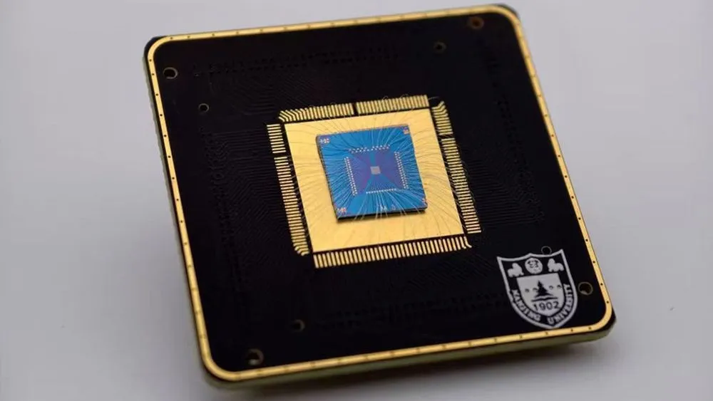
A research team including scientists from Nanjing University has reported a prototype chip called "LightTok" that generates data for image-recognition AI directly inside the sensor that captures light, according to a peer-reviewed paper published August 19.
In conventional systems, an image sensor first reads out pixel data, and a separate circuit then converts that data into a format AI models can process. LightTok moves part of this preprocessing step into the imaging device itself.
According to the research team, this approach can reduce the energy required for tokenization by roughly a factor of 14 compared to conventional methods. However, this figure does not represent power consumption measured on an actual device, such as a drone equipped with LightTok. It's important to distinguish between what was actually verified with the prototype chip and what was estimated based on projections for a larger-scale circuit.
Generating AI-Ready Data at the Point of Light Capture
Vision Transformers (ViT), used in image recognition, divide an image into small patches and convert each one into a sequence of numbers before processing. This numerical representation of each patch is what's referred to here as a "token." This differs from the tokens handled by text-generation AI, which represent words or character fragments.
In a typical setup, signals from each pixel are first read out from the image sensor as digital data. A separate computing circuit then divides the image into small patches and performs a transformation known as "patch embedding."
At the core of LightTok is a floating-gate phototransistor built from a single layer of molybdenum disulfide (MoS₂).
Each element responds to light and retains that information as an electrical state. Peripheral addressing circuitry selects pixels and applies voltages corresponding to pre-trained weights, summing the current flowing through each element to obtain an embedding value for each patch.
Light itself is not directly converted into a digital "token." Rather, information derived from light is held within the device, processed through analog circuitry, and only the final output is digitized.
The idea of performing computation inside the sensor itself is not new. The paper cites prior work, including image-processing chips built on two-dimensional semiconductors and imaging devices using single-layer MoS₂.
What LightTok aims to achieve is generating the patch embeddings fed into a ViT directly at the point of image capture. If all pixel data no longer needs to be sent outside the sensor before undergoing the same processing, power consumption associated with data transfer could potentially be reduced.
What the 32×32-Pixel Prototype Actually Demonstrated
The photosensitive memory array built by the research team consists of 32×32 pixels, totaling 1,024 elements.
In the paper's supplementary materials, a 3×3-pixel subset was used to perform weighted summation, with the results compared against values calculated on a computer. A binarized image of an airplane from the CIFAR-10 image classification dataset was used as the input example.
This experiment demonstrated that computation equivalent to patch embedding can be performed on the circuit. However, it does not constitute proof that the system can process high-resolution video in real time.
The number of gray levels in the input also matters significantly.
If only black-and-white binary values can be distinguished, substantial information about object shape and shading is lost. The research team experimentally demonstrated that light input can be handled across 41 distinct levels.
The supplementary materials further compare, using 256-level input as the reference, how much the resulting tokens differ. This comparison was conducted under conditions where a representative image was resized to 224×224 pixels and divided into 196 patches of 16×16 pixels each.
Results processed at 41 levels were closer to the 256-level reference than results using binary (2-level) input.
However, the 224×224-pixel figure refers to the image size used for simulation and comparison purposes. It does not mean the 32×32-pixel prototype array itself was scaled up to 224×224 pixels.
The paper's abstract reports that image classification using CIFAR-10 achieved accuracy close to that of software-based processing.
However, real drone footage involves moving targets, sudden changes in brightness, motion blur from vehicle vibration, and small distant objects. The test results published so far do not demonstrate that comparable recognition accuracy can be maintained under such conditions.
What Drove the "14.3x" Difference
The 14.3x figure results from comparing the tokenization process—one dot-product operation applied to a 16×16-pixel patch—under matched conditions of 41-level input precision and 4-microsecond processing time.
In the paper's supplementary materials, energy for the LightTok-type physical tokenizer is estimated including peripheral circuitry and digital conversion of the output. The conventional method, meanwhile, includes the process of transferring data from a CMOS image sensor to a separate computing circuit.
The ViT computation itself, which is common to both approaches, is not included in this comparison.
| One dot product for one 16×16-pixel patch | LightTok-type | Conventional digital method |
|---|---|---|
| Estimated energy for tokenization process | 1,743.9 pJ | 24,918.4 pJ |
| Of which: data transfer from sensor to compute circuit | Not applicable | 19,225 pJ |
| Input precision / processing time | 41 levels / 4µs | 41 levels / 4µs |
The source is Note 5 of the paper's supplementary materials. Dividing 24,918.4 by 1,743.9 yields approximately 14.3.
Additionally, the 19,225 pJ estimated for data transfer in the conventional method accounts for approximately 77.2% of that method's total energy consumption.
However, this 19,225 pJ figure was not measured by actually connecting an image sensor to a computing chip. It is an estimate derived from output-circuit simulation results, applying a condition of 50% bit-switching rate.
In the conventional method, signals from each pixel must first be read out, and the 256 pixels' worth of data within a patch must then be digitized.
The supplementary materials' estimate also allocates energy consumption to components such as the readout amplifier, current source on the image-sensor side, and circuitry that converts pixel signals into numerical values. Even summed together, these amounts remain smaller than the energy required for data transfer.
By contrast, the LightTok-type approach sums the signals from 256 pixels within the circuit itself, and only the resulting value is digitized.
Light itself is not generating power. What drives the large difference is the reduced number of pixel readouts, data transfers, and digital conversions required.
It's also worth noting that this isn't simply a case of subtracting the data-transfer cost to derive the new method's benefit—both methods are compared under conditions that include their respective peripheral circuitry.
The 1,743.9 pJ figure for the LightTok-type method is likewise not a simple sum of values measured directly on the prototype.
The research team applied the 4-microsecond current-stabilization time measured in the 3×3-pixel experiment to the processing time assumed for an integrated 16×16-pixel array. Energy consumption for peripheral circuitry was calculated by combining component specifications, circuit simulations, and conversions based on circuit capacitance.
The conventional method was likewise evaluated under the same conditions: a 4-microsecond processing time and 41-level input precision.
Therefore, while the 14.3x figure is meaningful as a design-level comparison under matched conditions, it is not the result of measuring two completed devices side by side.
A 41-level input corresponds to approximately 5.36 bits of information. Accordingly, the readout side of the conventional method was also configured with equivalent precision.
The supplementary materials separately estimate a scenario assuming 256-level input, equivalent to 8 bits. Under this condition, the conventional method faces a greater burden from digital conversion and data transfer, and the difference between the two methods grows to 20.5x.
The ratio changes because input precision and circuit conditions change.
Therefore, figures like 14.3x and 20.5x are not fixed performance differences that can be directly applied to any image-processing task or physical device.
The unit of comparison also deserves clarification.
Dividing a 224×224-pixel image into 16×16-pixel segments yields 196 patches. The supplementary materials present, as an example configuration, generating a 768-element embedding vector from each patch.
The pJ values shown in the table represent the energy required for a single dot-product operation to compute one of those 768 elements. They do not represent the total energy consumed by the entire system from image capture through to the final recognition result.
What Must Still Be Verified Before This Reaches a Drone
A significant gap remains between the 32×32-pixel prototype array and the envisioned system that would process 224×224-pixel images using 16×16-pixel patches.
First, it must be confirmed whether individual molybdenum disulfide elements continue to operate uniformly as pixel counts increase. Additionally, it must be verified whether the expected processing speed and power consumption can be achieved once wiring and peripheral circuitry are integrated at large scale.
Beyond that, accuracy and power consumption need to be compared against existing imaging systems while performing the same image-recognition tasks, using continuous images or video captured outdoors.
A drone's flight time is not determined solely by AI inference processing. Communication equipment, sensors, motors, and other components across the entire aircraft consume power.
Therefore, how much the energy savings achieved in the tokenization process would actually extend flight time can only be determined by measurements taken with the system integrated into an entire drone.
What LightTok has demonstrated so far is a specific circuit approach for shifting image-to-AI preprocessing onto the sensor itself, along with the potential to reduce the burden of data transfer as a result.
What's needed next is to operate the same mechanism at larger array scales and demonstrate actual image-recognition accuracy alongside whole-system power consumption simultaneously.