

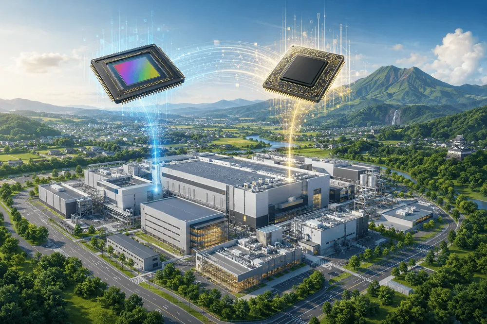
Sony Semiconductor Solutions (hereafter, Sony) and Taiwan Semiconductor Manufacturing Company (TSMC), the world's largest semiconductor foundry based in Taiwan, signed a memorandum of understanding (MOU) on May 8, 2026, regarding a strategic partnership aimed at developing and manufacturing next-generation image sensors. At the core of this partnership is the establishment of a new joint venture (JV) between the two companies. Under the agreed framework, Sony will hold a majority stake in the JV and retain management control, with plans to set up development and production lines at Sony's new fab (manufacturing plant) currently under construction in Koshi City, Kumamoto Prefecture.
Sony has long maintained an overwhelming top share of the market for CMOS image sensors used in mobile devices such as smartphones, effectively setting the industry standard in image processing technology. However, the market environment in recent years has become extremely fluid and competitive. In particular, rival Samsung Electronics of South Korea has been expanding its share—including within Apple's iPhone supply chain—backed by aggressive technology development and price competitiveness, putting increasing pressure on Sony's market dominance day by day. Against this backdrop of intensifying competition, Sony's decision not to cling to its own standalone vertically integrated model, but instead to directly incorporate TSMC's world-class foundry process technology and large-scale manufacturing expertise, is an extremely rational one.
In addition to new investment through the joint venture, the two companies are also proceeding in parallel with discussions on new capital investment at Sony's existing Nagasaki plant. These large-scale capital expenditures are planned to be executed in phases based on a meticulous analysis of market demand trends, while also being premised on securing public support from the Japanese government, as discussed below. The integration of technological resources through the joint venture represents an important strategic move for Sony to simultaneously achieve dramatic performance improvements in next-generation sensors and optimize manufacturing costs, thereby rebuilding its competitiveness.
The Rise of "Physical AI" and the Background Demanding Advanced Sensing
One particularly noteworthy aspect of this MOU is that the two companies have set their collaborative target on the field of "Physical AI." This includes automotive (autonomous driving) and advanced industrial/service robotics. Following the dramatic transformation that generative AI and large language models (LLMs) brought to information processing paradigms in cyberspace, the next technological frontier is shifting toward domains where AI directly interacts with the physical real world.
For AI systems to perceive the real world and make autonomous judgments, the performance of image sensors as the "eyes" that capture visual information from the outside world becomes a critical constraint. For autonomous driving systems to instantly judge complex traffic situations, wide dynamic range capable of handling extreme contrasts between light and dark, as well as low-latency, high-resolution sensing technology that captures fast-moving objects without blur, are indispensable. Similarly, robotic arms operating in factories and logistics hubs also require advanced visual data to recognize and grasp objects with millimeter-level precision.
Sony President and CEO Shinji Sashida commented on the partnership, stating that it is "an important initiative that brings together the strengths of both companies, driving further advancement of technology and business in the field of next-generation image sensors," expressing his determination to create new markets through unique technology. Echoing this sentiment, TSMC Senior Vice President and Deputy Co-COO Kevin Zhang positioned the collaboration as "an important step toward leading the future of sensing technology in the AI era," emphasizing the shared vision of both companies toward delivering innovative solutions. As AI continues to evolve, the fusion of advanced data processing on edge devices with highly capable sensors is an inevitable trend, and this partnership directly addresses that demand.
TSMC's Japan Strategy and the Aim of Securing an Anchor Customer
Analyzing this partnership from TSMC's perspective reveals two important motivations: business expansion in Japan and establishing a foothold in a growth market. TSMC has already built its first fab in Kikuyo Town, Kumamoto Prefecture, beginning mass production in late 2024. This plant plays a role in stably supplying logic semiconductors ranging from mature 22/28nm and 12/16nm processes to mid-end nodes for Sony and major automotive parts supplier Denso. Furthermore, there are observations suggesting that the introduction of a 3nm process is also being considered for the construction of a second fab, underscoring the growing importance of TSMC's manufacturing presence within Japan.
For TSMC, this joint venture offers an opportunity to firmly secure Sony—the industry's top player—as a stable, long-term anchor customer in the image sensor field, a domain with different strengths from TSMC's own logic semiconductors. By taking a minority stake, TSMC can limit the financial risk associated with massive capital investment while enabling deep co-optimization between Sony's sensor design technology and TSMC's cutting-edge process technology.
In particular, hardware for physical AI is likely to face an explosive demand cycle over the next several years. As image sensors come to be positioned as core infrastructure for AI perception systems, securing collaboration on next-generation manufacturing processes at this stage is an extremely effective move to ensure capturing the fruits of future market expansion. Beyond merely providing manufacturing capacity as a foundry, by deepening the partnership from the design stage, TSMC is seeking to establish an overwhelming advantage even in the sensor market, which demands specialized requirements.
Strengthening the Semiconductor Supply Chain in Tandem with National Strategy
Another critical factor underpinning the feasibility and business stability of this partnership is the strong backing from the Japanese government. The MOU explicitly states that the establishment of the joint venture and its investment plans are premised on support from the Japanese government. In recent years, semiconductors have gone beyond being mere industrial infrastructure, becoming positioned as the most critical materials for economic security at the core of national strategies worldwide. The Japanese government, particularly the Ministry of Economy, Trade and Industry (METI), has set forth a policy of injecting massive public funds toward rebuilding domestic semiconductor supply chains and securing manufacturing capacity.
According to reports, METI has reportedly already decided on a policy to provide subsidies of up to 60 billion yen (approximately $380 million) for the construction of Sony's new image sensor plant in Kumamoto. The global trend of allied nations promoting the reshoring of semiconductor manufacturing and diversifying production bases is accelerating worldwide, and this represents a perfect alignment between the national policy of forming a robust ecosystem within Japan and corporate needs for stable production bases for advanced technology.
The strengthened collaboration between Sony and TSMC goes beyond the framework of individual corporate business strategies, solidifying the status of Kyushu and Kumamoto as a "Silicon Island" and generating momentum that drives Japan's entire advanced semiconductor ecosystem forward. While the MOU currently remains at a legally non-binding stage, with procedures such as final contract execution and approval processes from regulatory authorities in various countries still remaining, given the clear tailwind of government support, the path toward commercialization is generally expected to proceed smoothly. Toward the practical application and widespread adoption of physical AI, the development race for image sensor technology responsible for perception has entered a new dimension that now involves national strategy as well.