サイエンス
「2次元でも3次元でもない」炭素の隙間に潜む未知の量子状態を初観測
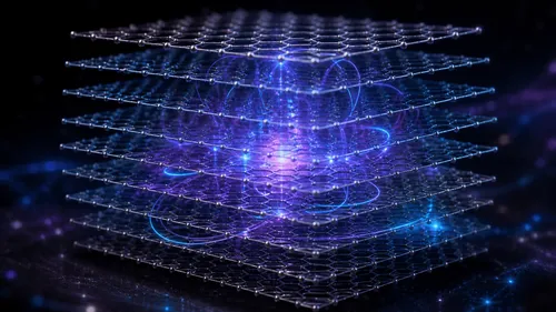
国際研究チームが、極薄の菱面体積層グラフェンにおいて、電子が2次元と3次元の運動を同時に保つ「次元横断的異常ホール効果」を初めて実験的に実証した。この発見は、電子の磁化と電流、ホール電場の直交関係という従来の物理学の常識を覆し、量子物質科学の新たなパラダイムを切り開くものだ。
南京大学の物理学教授。グラフェンをはじめとする原子層物質の高品質デバイス作製と、極限環境下での量子輸送測定を専門とする。本研究において、9層グラフェンデバイスの精密な制御と異常ホール効果の観測に大きく貢献した。
Superlattices have attracted great interest because their use may make it possible to modify the spectra of two-dimensional electron systems and, ultimately, create materials with tailored electronic properties. In previous studies (see, for example, refs 1, 2, 3, 4, 5, 6, 7, 8), it proved difficult to realize superlattices with short periodicities and weak disorder, and most of their observed features could be explained in terms of cyclotron orbits commensurate with the superlattice. Evidence for the formation of superlattice minibands (forming a fractal spectrum known as Hofstadter’s butterfly) has been limited to the observation of new low-field oscillations and an internal structure within Landau levels. Here we report transport properties of graphene placed on a boron nitride substrate and accurately aligned along its crystallographic directions. The substrate’s moiré potential acts as a superlattice and leads to profound changes in the graphene’s electronic spectrum. Second-generation Dirac points appear as pronounced peaks in resistivity, accompanied by reversal of the Hall effect. The latter indicates that the effective sign of the charge carriers changes within graphene’s conduction and valence bands. Strong magnetic fields lead to Zak-type cloning of the third generation of Dirac points, which are observed as numerous neutrality points in fields where a unit fraction of the flux quantum pierces the superlattice unit cell. Graphene superlattices such as this one provide a way of studying the rich physics expected in incommensurable quantum systems and illustrate the possibility of controllably modifying the electronic spectra of two-dimensional atomic crystals by varying their crystallographic alignment within van der Waals heterostuctures.
A decade of intense research on two-dimensional (2D) atomic crystals has revealed that their properties can differ greatly from those of the parent compound. These differences are governed by changes in the band structure due to quantum confinement and are most profound if the underlying lattice symmetry changes. Here we report a high-quality 2D electron gas in few-layer InSe encapsulated in hexagonal boron nitride under an inert atmosphere. Carrier mobilities are found to exceed 103 cm2 V-1 s-1 and 104 cm2 V-1 s-1 at room and liquid-helium temperatures, respectively, allowing the observation of the fully developed quantum Hall effect. The conduction electrons occupy a single 2D subband and have a small effective mass. Photoluminescence spectroscopy reveals that the bandgap increases by more than 0.5 eV with decreasing the thickness from bulk to bilayer InSe. The band-edge optical response vanishes in monolayer InSe, which is attributed to the monolayer's mirror-plane symmetry. Encapsulated 2D InSe expands the family of graphene-like semiconductors and, in terms of quality, is competitive with atomically thin dichalcogenides and black phosphorus.
Impact ionization, which supports carrier multiplication, is promising for applications in single photon detection1 and sharp threshold swing field effect devices2. However, initiating the impact ionization of avalanche breakdown requires a high applied electric field in a long active region, which hampers carrier multiplication with a high gain, low bias and superior noise performance3,4. Here we report the observation of ballistic avalanche phenomena in sub-mean free path (MFP) scaled vertical InSe/black phosphorus (BP)5–9 heterostructures10. We use these heterojunctions to fabricate avalanche photodetectors (APDs) with a sensitive mid-infrared light detection (4 μm wavelength) and impact ionization transistors with a steep subthreshold swing (<0.25 mV dec–1). The devices show a low avalanche threshold (<1 V), low noise figure and distinctive density spectral shape. Our transport measurements suggest that the breakdown originates from a ballistic avalanche phenomenon, where the sub-MFP BP channel support the lattice impact ionization by electrons and holes and the abrupt current amplification without scattering from the obstacles in a deterministic nature. Our results provide new strategies for the development of advanced photodetectors1,11,12 via efficient carrier manipulation at the nanoscale.Ballistic avalanche phenomena in vertical InSe/BP heterostructures enable the demonstration of high-performance avalanche photodetectors and impact ionization transistors.
Graphene enables precise carrier-density control via gating, making it an ideal platform for studying electronic interactions. However, sample inhomogeneities often limit access to the low-density regimes where these interactions dominate. Enhancing carrier mobility is therefore crucial for exploring fundamental properties and developing device applications. Here, we demonstrate a significant reduction in external inhomogeneity using a double-layer graphene architecture separated by an ultra-thin hexagonal boron nitride layer. Mutual screening between the layers reduces scattering from random Coulomb potentials, resulting in a quantum mobility exceeding 107cm2V−1s−1\documentclass[12pt]{minimal} \usepackage{amsmath} \usepackage{wasysym} \usepackage{amsfonts} \usepackage{amssymb} \usepackage{amsbsy} \usepackage{mathrsfs} \usepackage{upgreek} \setlength{\oddsidemargin}{-69pt} \begin{document}$$1{0}^{7}{{\rm{c}}}{{{\rm{m}}}}^{2}{{{\rm{V}}}}^{-1}{{{\rm{s}}}}^{-1}$$\end{document}. Shubnikov–de Haas oscillations emerge at magnetic fields below 1 mT, while integer quantum Hall features are observed at 0.002 T. Furthermore, we identify a fractional quantum Hall plateau at a filling factor of vtot=−10/3\documentclass[12pt]{minimal} \usepackage{amsmath} \usepackage{wasysym} \usepackage{amsfonts} \usepackage{amssymb} \usepackage{amsbsy} \usepackage{mathrsfs} \usepackage{upgreek} \setlength{\oddsidemargin}{-69pt} \begin{document}$${v}_{{{\rm{tot}}}}=-10/3$$\end{document} at 2 T. These results demonstrate the platform’s suitability for investigating strongly correlated electronic phases in graphene-based heterostructures. Enhancing the carrier mobility of graphene can enable the investigation of its fundamental properties and promote device applications. Here, the authors report the fabrication of double-layer graphene devices with a quantum mobility up to 107 cm2V−1s−1 and integer quantum Hall features at magnetic fields as low as 0.002 T.
The coupling of ferroelectricity and magnetic order provides rich tunability for engineering material properties and demonstrates great potential for uncovering novel quantum phenomena and multifunctional devices. Here, we report interfacial ferroelectricity in moiré superlattices constructed from graphene and hexagonal boron nitride. We observe ferroelectric polarization in an across-layer moiré superlattice with an intercalated layer, demonstrating a remnant polarization comparable to its non-intercalated counterpart. Remarkably, we reveal a magnetic-field enhancement of ferroelectric polarization that persists up to room temperature, showcasing an unconventional amplification of ferroelectricity in materials lacking magnetic elements. This phenomenon, consistent across devices with varying layer configurations, arises purely from electronic rather than ionic contributions. Furthermore, the ferroelectric polarization in turn modulates quantum transport characteristics, suppressing Shubnikov-de Haas oscillations and altering quantum Hall states in polarized phases. This interplay between ferroelectricity and magneto-transport in non-magnetic materials is crucial for exploring magnetoelectric effects and advancing two-dimensional memory and logic applications. The coupling of ferroelectricity and magnetic order enables the tunability of material properties. Here, authors realize magnetic-field-enhanced ferroelectricity and electrical-field-controlled magneto-transport in non-magnetic moiré superlattices.