


With the explosive spread of generative AI, data center cooling systems are being pushed to run at full capacity, and to process and store the enormous volumes of data we generate every day, modern digital society continues to discard staggering amounts of electric power as "heat." Current semiconductor memory must constantly supply power to maintain stored information, and it faces a structural limitation in which heat generation increases exponentially as operating frequency rises. As a fundamental hardware-level solution to this energy problem, non-volatile magnetic memory (MRAM)—which stores information not through the presence or absence of electric charge but through the "direction of magnetization"—is being actively developed.
Conventional MRAM has used "ferromagnets," which share the same properties as ordinary magnets, as the recording layer. Because ferromagnets generate stray magnetic fields externally, when memory elements are packed together at the nanoscale, their magnetic fields interfere with each other and corrupt data. Furthermore, due to the physical limits of the dynamics involved in reversing ferromagnetic magnetization, operating speed has been constrained by a nanosecond (one billionth of a second) barrier.
The next-generation material that has emerged at the forefront of research to break through this barrier is the "antiferromagnet." In antiferromagnets, the spins (a property analogous to rotation) of internal electrons align in opposing directions and cancel each other out, so the material as a whole has no net magnetization and produces no stray magnetic field externally. This allows elements to be packed together at extremely high densities. Moreover, because the spin dynamics of antiferromagnets have intrinsic frequencies in the terahertz range, ultrafast operation on the picosecond (one trillionth of a second) scale—two to three orders of magnitude faster than ferromagnets—is theoretically possible.
Among these materials, an alloy of manganese and tin known as a "chiral antiferromagnet" () has attracted particular attention as an ideal recording material. Despite being an antiferromagnet, it exhibits electrical responses such as the anomalous Hall effect, making its magnetic state easy to read out.
The Limits of the "Melt with Heat, Then Solidify" Process That Delays Switching
To electrically control the magnetic order of , a technique called spin-orbit torque (SOT) is used. This approach involves running an electric current through a heavy-metal layer, such as tantalum (), placed adjacent to the layer, and injecting the resulting "spin current" (a flow of spin angular momentum) into the layer to directly flip the spin orientation.
At first glance, this method appears capable of achieving ultrafast direct writing on the picosecond scale. However, in real devices, "Joule heating"—which inevitably occurs whenever current flows—stands in the way. When a large current pulse is injected into the heavy-metal layer, the temperature of the device rises sharply. If this heat exceeds the limiting temperature at which can maintain its magnetic order (the Néel temperature, approximately ), the aligned spins become disordered and the stored information is temporarily lost.
As the device cools after the current pulse ends, magnetic order re-forms in a new direction depending on the polarity of the spin current. This process is known as the "thermally assisted mechanism."
Writing via the thermally assisted mechanism closely resembles a blacksmith's work: heating iron until it becomes soft, shaping it, and then cooling it to solidify the new form. While this reliably changes the shape, it requires waiting through the processes of heat generation and cooling. This thermal relaxation takes 100 nanoseconds or more, fundamentally negating the picosecond-scale ultrafast dynamics that antiferromagnets inherently possess. What we truly want is switching via an "intrinsic mechanism," in which a single precise hammer blow (the spin current) instantaneously reverses the structure at room temperature. So how can we eliminate the influence of Joule heating and draw out this intrinsic mechanism?
The 30-Nanometer Boundary—How a Precisely Engineered Interface Unlocked Non-Thermal Switching
A research team led by the University of Tokyo and Keio University has presented a simple yet powerful answer to this question: "optimizing heat dissipation through control of device film thickness."
The team fabricated multilayer films of and on a silicon substrate using sputtering. In this process, all layers—including an alumina () capping layer to prevent oxidation—were deposited at room temperature, followed by an annealing treatment at . Observations using transmission electron microscopy (TEM) and atomic force microscopy (AFM) confirmed that the roughness of the interface between and was suppressed to just $0.5$–$0.6\text{ nm}$, indicating that an extremely high-quality, smooth interface was formed—smoother than those reported in prior studies. This atomic-level smoothness enables highly efficient injection of spin current from the heavy-metal layer into the antiferromagnetic layer.
X-ray diffraction structural analysis showed that even as the film was thinned, the tendency of the crystal structure (the kagome plane) to stand perpendicular to the film surface (out-of-plane orientation) was maintained. This made it possible to accurately evaluate the film-thickness dependence of the SOT switching current density () while excluding noise arising from differences in crystallinity, as the thickness $t$ of the magnetic recording layer was varied from to .
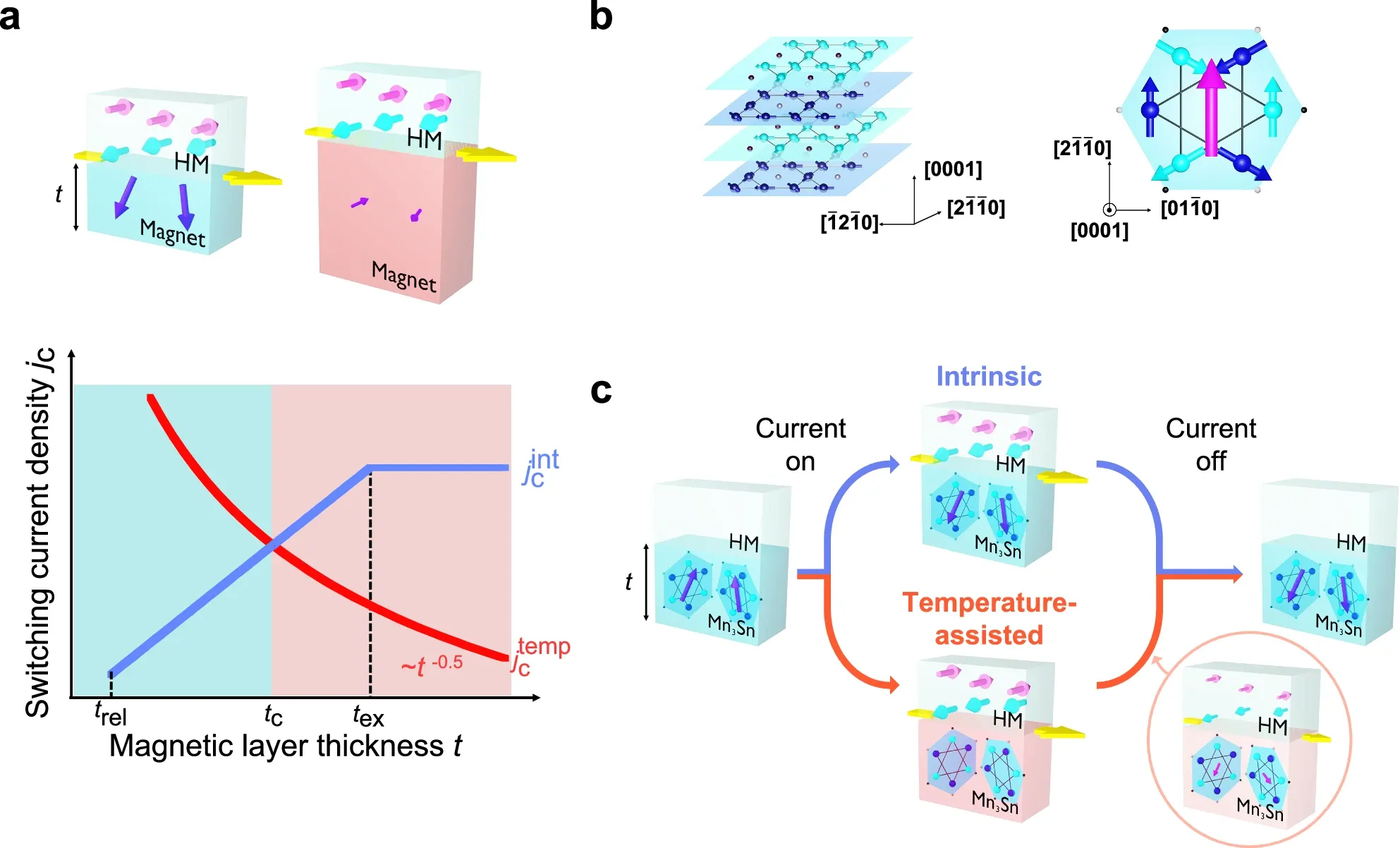
Measurements revealed that in devices with thicker layers, heat generated by the current tends to accumulate inside the device, and in the region where the film thickness exceeds approximately , was found to scale with film thickness $t$ according to a power law. This scaling law is in complete agreement with theoretical predictions for the thermally assisted mechanism, in which writing occurs once the device reaches the Néel temperature.
When the film thickness was reduced below , the situation changed dramatically. The generated Joule heat was efficiently dissipated into the substrate, suppressing the rise in device temperature. The current density required for switching began to deviate significantly from the curve and decreased. The metric for power required for switching also showed a clear declining trend in the thinner region, with as the boundary.
These data indicate that the dominant switching mechanism shifts at a boundary of film thickness . In thinner devices, the torque from the injected spin current overcomes the magnetic order and directly reverses the state before the device temperature reaches the Néel temperature and magnetic order collapses. This represents a crossover to a truly "intrinsic mechanism" driven solely by the force of the spin current.
| Comparison item | Thermally assisted mechanism (thick film) | Intrinsic mechanism (thin film: this study) |
|---|---|---|
| Writing process | Magnetic order is destroyed by heat and reconstructed during cooling | Spin current directly reverses magnetic order |
| Rate-limiting step | Time required for heat generation and cooling | Spin current injection and magnetic dynamics |
| Estimated switching time | ~100 nanoseconds or more | Tens of picoseconds to a few nanoseconds |
| Magnetic order during operation | Temporarily lost due to Joule heating | Maintained from room temperature |
| Approximate Mn3Sn film thickness | Exceeds | or less |
A 10-Nanosecond Single Pulse Proves the Superiority of "Direct Writing"
In the thin-film regime where the intrinsic mechanism dominates, how far can the inherent high speed of antiferromagnets be pushed? The research team conducted an experiment using the thinnest device, progressively shortening the width (duration) of the applied current pulse.
Prior studies had shown that when the thermally assisted mechanism is at work, the signal strength required for switching decays sharply once the pulse width is shortened below a few tens of a microsecond (a few hundred nanoseconds), because time is needed to heat and cool the device.
With the device, the magnitude of the electrical signal accompanying switching (the anomalous Hall voltage) remained largely unchanged even as the pulse width was varied from an extremely long (milliseconds) down to an ultrashort (nanoseconds). The most striking result was that a single short pulse (current density ) applied just once was sufficient to achieve full reversal.
This result provides strong evidence that magnetic order is instantaneously rewritten while the current pulse is being applied, without waiting for the device to cool. The superiority of the heat-independent intrinsic mechanism has been demonstrated as a clear observational fact.
The Power of "Polycrystalline" Films and the Path Toward Mass Production and Social Implementation
The industrial value of this research extends beyond demonstrating ultrafast operation. Notably, the material used in the experiments was not a special single-crystal (epitaxial) film but a "polycrystalline film" deposited by sputtering onto a common silicon wafer.
Until now, it had been believed that highly efficient SOT switching required high-quality epitaxial films with precisely aligned orientation. Epitaxial growth has the drawback of severely restricting the choice of substrate material, making integration with existing silicon semiconductor processes difficult. This new device design achieves intrinsic switching at current densities equal to or lower than those reported for epitaxial systems, while using a polycrystalline film that is highly compatible with mass-production processes. This serves as a decisive passport for antiferromagnetic memory to move beyond laboratory showcases and onto actual semiconductor foundry manufacturing lines.
In the current device structure, a small external assist magnetic field (bias field) is applied to determine the switching direction. Going forward, integrating field-free switching technology—which requires no external magnetic field at all, through approaches such as introducing asymmetry into the device structure—will become an urgent task. In actual memory chips, device sizes will shrink dramatically from the current micrometer scale to the nanometer scale, so verifying scaling behavior in nanodevices, taking into account further reductions in heat capacity and changes in thermal boundary resistance, will also be a next step.
When this new design is ultimately implemented in society, its impact will be immense. Antiferromagnetic MRAM, with its ultrafast speed and extremely low power consumption, could be directly integrated as large-capacity cache within next-generation processors handling AI training and inference. The current abnormal infrastructure, which pours enormous amounts of electricity and fresh water into cooling massive data centers, could be fundamentally improved, dramatically reducing both operating costs and environmental impact.
The landscape of the devices we hold in our hands would also change. Because information is retained even when the power is turned off, standby power consumption would become effectively zero while still processing large volumes of data instantaneously. Smartphones might need charging only once every few days, and edge AI devices capable of sophisticated processing without a network connection could be deployed everywhere throughout our cities.
Deep within the computers we use, electron spins would continue to reverse precisely and coolly on the picosecond scale, undisturbed by heat. The timeline toward such ultimate hardware has now been decisively rewritten by this discovery of the "30-nanometer boundary."