


On September 8, 2026, Arm announced the "Neoverse CSS N4," aimed at data centers. Customers can choose from 8 to 128 Neoverse N4 cores per die, and it is the first N-series compute subsystem to support up to 3.8GHz clock speeds, LPDDR6, and PCIe Gen 7. But this is not a new finished CPU made by Arm. It is a design foundation that has already assembled and verified CPU cores, interconnects, memory and I/O peripheral circuitry, management functions, and software—customers then add their own features on top to build their own silicon. Behind the headline figure of up to 128 cores lies a shifting division of labor over how much of CPU development Arm itself now handles.
Before the 128 cores, how deeply is the CSS already built out?
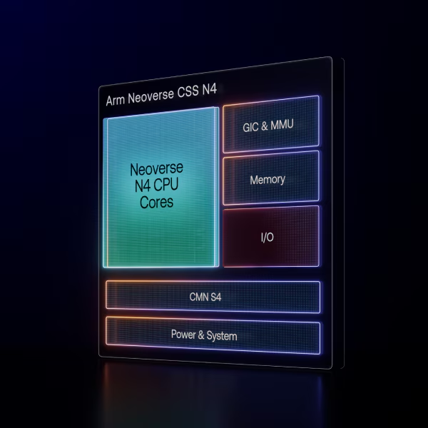
The Neoverse CSS N4 is not a product where customers simply license a standalone CPU core. According to Arm, it pre-integrates the Neoverse N4 core, the CMN mesh interconnect, system IP such as interrupt control and memory management, and power and system management. Arm delivers this as RTL-format design data that customers can import directly into modern EDA tools. Along with implementation guidance and support for third-party IP interoperability, it also comes with integrated software that lets customers boot Linux and begin verification and software development right away.
RTL is a stage that describes the behavior of logic circuits—it is neither manufacturing data ready to hand to a fab nor a packaged CPU. Even so, it shifts to Arm's side the work of integrating and verifying the interconnect, management circuitry, and boot software that customers would otherwise have to handle themselves when starting from individual CPU core IP. This frees customer engineers to spend more time on proprietary accelerators, memory and I/O, chiplet configurations, and power/performance tuning for specific applications.
The CSS framework itself is not new. Arm introduced it in early 2023, and says the previous generation of Neoverse CSS has already been used in Microsoft's cloud CPUs and DPUs for network processing. What's changed with N4 is that, while preserving a highly finished starting point, Arm has expanded the core count range from 8 to 128 and broadened the choices available for cache, memory, I/O, accelerator connections, and chiplet interconnects.
More cores, cache, and I/O built on N3P
The maximum configuration numbers clearly reflect the use cases N4 is targeting. According to specifications reported by Tom's Hardware based on Arm's briefing materials, each core can have 64KB of L1 instruction cache and 64KB of L1 data cache, plus up to 2MB of L2 cache, while the die as a whole can be configured with up to 256MB of shared L3 cache. Memory support includes DDR5 or LPDDR6, and I/O supports up to 128 lanes of PCIe 6/7 and CXL 4.0. The design also anticipates scaling across multiple dies or sockets using UCIe for chip-to-chip connections.
| Published maximum specs | Neoverse CSS N2 | Neoverse CSS N4 |
|---|---|---|
| CPU cores/die | 64 | 128 |
| L2 cache/core | 1MB | 2MB |
| Shared cache/die | 64MB | 256MB |
| Memory | DDR5, LPDDR5 | DDR5, LPDDR6 |
| PCIe/CXL | PCIe/CXL Gen5, 4×16 lanes | PCIe 6/7, up to 128 lanes, CXL 4.0 |
This table shows the generational differences in published maximum values—it is not a performance comparison normalized for the same power consumption or die area. Notably, Arm chose CSS N3, not N2, as the performance comparison target for N4. Compared to N2, core count doubled from 64 to 128, L2 per core doubled from 1MB to 2MB, and shared cache quadrupled from 64MB to 256MB—but there's no guarantee these maximum values would all be adopted simultaneously in a single product.
The same caution applies to the 3.8GHz maximum clock speed. Arm has not disclosed which configuration among the 8-to-128-core range actually reaches this top frequency. Whether to add more cores or raise the clock speed, and how much area and power to allocate to cache and memory bandwidth, are interrelated trade-offs. The value of CSS N4 lies not in maxing out every spec simultaneously, but in the ability to shift the allocation to suit different use cases—cloud CPUs, DPUs, or networking equipment.
The manufacturing process also requires a caveat. Arm's performance comparison slides list CSS N4 on TSMC's N3P and CSS N3 on 5nm. Meanwhile, Digital Today reported that an Arm representative at a media briefing said N3 and N3P are the main design candidates, and that there is also demand for Samsung's SF2 and SF2P. N3P is at least the reference implementation for the performance claims, but it is not a fixed name that determines the manufacturing destination for every product customers build.
Reading the caveats behind "up to 2x" and development-time reductions
Arm claims up to 2x per-socket performance, up to 1.25x performance-per-watt, and up to 1.75x memory bandwidth compared to CSS N3. According to footnotes on the announcement slides, these figures compare a maximum-core-count configuration at 3GHz with 2MB of L2 cache per core, pitting the 5nm N3 against N4 on N3P. In other words, "up to 2x" does not mean that the instruction-processing performance of a single N4 core has doubled. It is a comparison of the entire socket, including core count, manufacturing process, and system configuration.
Information needed to fully judge these claims is still missing. Arm has not disclosed benchmark names, absolute performance figures, power consumption, or die area. The effects of increasing core count and moving to N3P cannot be separated. The 1.25x performance-per-watt figure indicates an efficiency improvement, but the results for a finished CPU will vary depending on the memory, I/O, and clock speed a customer chooses. At this stage, it's most appropriate to read these numbers as design targets under conditions Arm itself defined, rather than as guaranteed real-world results.
The development-time figures are similarly inconsistent. Arm describes the time reduction enabled by CSS as up to one year on its current product page, but up to roughly 24 months in its March 2026 investor materials—and it has not disclosed the specific reduction figure for N4 or the calculation basis for either number. A 2025 CSS explainer also mentioned reducing time to first working silicon by up to 12 months. It's unclear from each source what starting and ending points are used—design kickoff, prototype silicon, or market launch—or what conventional development approach is being assumed as the baseline. These maximum figures cannot be read as a general delivery-time guarantee.
From IP to finished CPU: Arm's offerings now span three tiers
Arm's product lineup now spans three tiers—CPU IP, integrated and verified CSS, and the finished-silicon Arm AGI CPU—and the amount of work customers must handle themselves decreases as they move toward the latter.
| What you get from Arm | Main work left to the customer | Best suited for |
|---|---|---|
| Neoverse CPU IP | Broadly designing the interconnect, management circuitry, memory/I/O, physical implementation, and software | Large-scale designers who want to strongly differentiate the entire CPU |
| Neoverse CSS | Building on integrated, verified RTL to add proprietary IP, configuration, physical implementation, manufacturing, and productization | Businesses that want proprietary silicon while limiting development time |
| Arm AGI CPU | Integrating a finished CPU into servers and optimizing the system and software | Businesses that want fast deployment without doing CPU design themselves |
This classification isn't about which tier offers superior performance—it's about who bears the design risk. The N-series CSS N4 emphasizes throughput per watt and per area, targeting scale-out workloads, networking, and DPUs. The Arm AGI CPU, which uses the V3 core, is a finished product for workloads that demand responsiveness. Although both share the same Neoverse software foundation, they serve different customers: those who want to customize the CPU to their own specifications, and those who simply want to buy a finished product.
For Arm, CSS functions both as technical support and as a product that raises the price per unit. Arm's March 2026 investor materials state that IP royalties for the CSS platform are twice those of standalone Armv9 IP. While Arm has not disclosed the specific contract fees or royalty rates for N4, the business logic is clear: by expanding its offerings beyond the CPU core itself, Arm increases the value it can capture from each customer chip.
However, as this middle tier expands, it also creates tension in customer choices. While using CSS reduces integration work, it deepens dependence on the configurations and roadmap that Arm has verified. Furthermore, Arm has now begun selling finished silicon through the AGI CPU. From a customer's perspective, the IP supplier, design partner, and finished-CPU vendor now overlap within the same company, making it necessary to draw a clear line—before signing any contract—between what constitutes their own area of differentiation and what they're willing to leave to Arm.
What's left for customers to design, and what to watch next
Adopting CSS N4 doesn't make CPU development disappear. Customers still choose core count and cache configuration to fit their use case, connect accelerators, and decide on memory and I/O. After that comes physical implementation, timing closure, power consumption tuning, tape-out, manufacturing, packaging, and system verification. Arm Total Design connects EDA companies, design firms, foundries, and firmware companies, but it is not a framework that shifts mass-production responsibility onto Arm itself.
Many details remain undisclosed. The adopting companies, timing of the first tape-out and samples, TDP and die area for a 128-core configuration, pricing, and measured workload results are all unknown. "Agentic AI" is also simply Arm's demand hypothesis—that AI agents will increase CPU-side processing through data retrieval and tool execution—not a measured figure showing how much CSS N4 speeds up any specific AI workload.
Whether the Neoverse CSS N4 succeeds will become clear not from its maximum specifications, but from which configurations customers actually choose, when they get silicon running, and how many months they manage to cut compared to conventional individual-IP design. Only once power consumption and performance figures for real products are published will it become possible to verify whether the division of labor Arm has redrawn can support both shorter design timelines and higher royalties at the same time.