

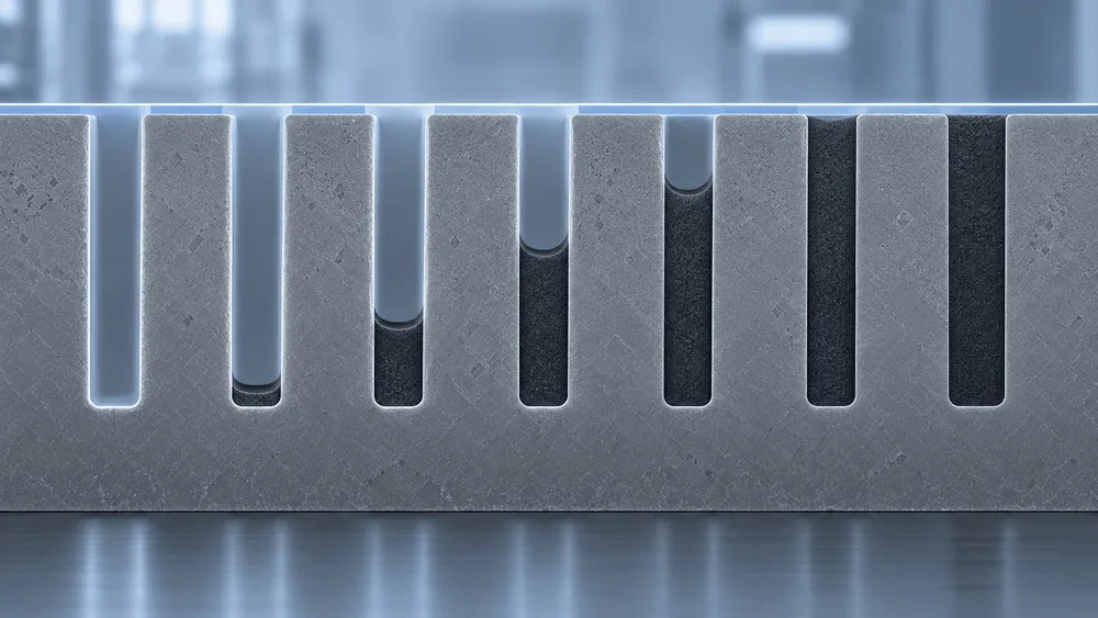
On September 22, Dutch semiconductor equipment maker ASM announced XP8 Vertos Flowable Carbon, a carbon film that fills fine trenches while leaving a flat surface.
Using plasma-enhanced chemical vapor deposition (PECVD), the technology aims to handle gap fill and planarization, which have often required separate processes, in a single deposition step. According to ASM, early adoption in volume production has already begun.
The technology did not appear out of nowhere in 2026, however. Three years ago, the company was already presenting, in public materials, a carbon film that could planarize the surface as it was deposited.
What matters most about this announcement is less the idea behind the new material than the fact that a technology once at the research and development stage is starting to be adopted as a product for volume production equipment.
Filling trenches while flattening the surface
As semiconductors become more three-dimensional, a growing number of steps involve filling narrow, deep trenches and holes with material and then building the next layer on top.
With conventional conformal carbon films, the material can coat the bottom and sidewalls of a trench, but the unevenness of the underlying structure tends to carry through to the film's surface.
If that unevenness is passed on to the upper layers, an additional planarization step is needed to create a flat surface suitable for the fine patterning that follows.
ASM's goal is to combine gap fill and planarization into one process.
According to the company, the new carbon film grows from the bottom of the trench upward, and the surface flattens as the film is deposited.
ASM says it can fill high-aspect-ratio structures, where depth is large relative to width, without leaving voids or seams inside the film.
ASM also emphasizes that the film can more easily even out surface height even when regions of different pattern density coexist on the wafer.
A semiconductor wafer contains areas where fine patterns are densely packed alongside areas with relatively wide open space. Even when a film of the same thickness is formed, the surface height can differ from place to place.
The planarization Vertos aims for is not only about filling a single trench cleanly, but also about maintaining a surface suitable for the next processing step across these differences in pattern density.
This could make it possible to omit some of the chemical mechanical polishing (CMP) and etch-back steps that were previously needed after deposition.
However, what may be omitted are the steps related to gap fill and planarization with this carbon film. It does not mean that all polishing steps used in semiconductor manufacturing, including CMP, become unnecessary.
Another way to fill uneven surfaces is spin-on carbon, in which a liquid material is applied to a rotating wafer to form a film.
In a comparison ASM presented in 2023, the company explained that this method may require additional processing to reduce excess film thickness and can be difficult to apply to some structures.
The novelty of this technology is not the use of carbon to fill trenches in itself.
It differs from both spin-on methods, which rely on the flow of a liquid material, and conventional carbon films that follow the underlying shape. Instead, it forms a flowable carbon film in a PECVD tool and performs gap fill and planarization at the same time.
| Method | Characteristics and challenges cited by ASM | Position in this announcement |
|---|---|---|
| Conventional conformal carbon film | Underlying unevenness remains on the surface, and correction may be needed in later steps | Comparison target in the 2026 announcement |
| Spin-on carbon | Depending on the structure, additional processing may be needed to reduce excess film thickness | Compared in ASM's 2023 materials |
| Vertos flowable carbon film | Fills trenches while flattening the surface, aiming to reduce some CMP and etch-back steps | Commercialized in 2026, with early adoption in volume production begun |
This table organizes the comparison targets ASM presented in materials from different periods.
It is not the result of a test that directly compared the yield or cost of the three methods using the same trench geometry, the same wafers, and the same manufacturing conditions.
The technology was shown as early as 2023
The announcement uses the phrase "market first," but that does not mean the underlying principle was discovered for the first time in 2026.
What ASM calls a first is offering a flowable carbon film formed by PECVD as a product for volume production tools.
The concept of a self-planarizing PECVD carbon film itself already appeared in investor materials the company published in 2023.
Following ASM's public materials reveals the course of development.
In 2023, it introduced self-planarizing PECVD carbon gap fill technology. In 2025, it published a cross-sectional image showing a void-free fill. Then, in September 2026, it announced the technology as a formal product and disclosed that early adoption in volume production had begun.
The sources are page 69 of the 2023 investor materials, page 10 of the 2025 materials, and the September 22, 2026 press release.
The 2023 materials showed "self-planarizing PECVD carbon gap fill" and explained how it differs from spin-on carbon.
The 2025 materials included a cross-sectional image described as "void-free" with "good planarity," and introduced the technology as one of the drivers for growing ASM's PECVD business.
However, none of these materials named a specific customer adopting it in volume production.
What is newly clear this time is that it has been formally launched as a product called XP8 Vertos Flowable Carbon and has progressed to early adoption in volume production.
That said, all of the materials so far were published by ASM itself.
Even the cross-sectional image shown in 2025 does not prove that the same performance can be achieved in every application, regardless of structure or manufacturing conditions.
As for early adoption in volume production, ASM has not disclosed which chipmaker is using it, in which product, or at what scale.
Applications in logic and memory patterning
Vertos carbon film has not been announced as a new conductive interconnect material or as a carbon-based transistor material.
ASM positions it as an auxiliary film used in the process of forming fine semiconductor patterns.
In advanced logic, it is expected to be applied to processes that use hardmasks.
A hardmask is an auxiliary film that withstands etching and preserves the processed shape when a fine pattern formed on an upper layer is transferred to the layers below.
For this reason, a flat surface after filling with the carbon film is important for creating even finer patterns on top of it.
ASM's product page lists targets ranging from narrow trenches to micrometer-scale cavities.
It also says the film can be used for patterning materials that control dipoles and work functions.
Use is not limited to filling a space completely.
According to ASM's technical explanation, after the carbon film is formed to the required height, a recess process can be performed in the same tool to adjust the film's height and shape.
If the required film thickness can be adjusted for each structure, it may become easier to set conditions for subsequent processing.
However, no data expressing such effects in numerical terms for each process has been published.
In memory, ASM envisions use in the deep structures of DRAM and 3D NAND.
The company says applications in advanced packaging and wafer-level integration technologies are still under consideration.
Meanwhile, all that can be confirmed from the September 22 announcement is that the product has reached the stage of "early adoption" in volume production.
This does not mean it has been broadly adopted in volume production across both logic and memory.
The breadth of anticipated applications and actual adoption need to be viewed separately.
More numbers are needed to judge the real impact
ASM says that by reducing additional CMP and etch-back steps, it can limit process complexity, cost, and the risk of defects.
The value of integrating processes depends on how far it actually reduces the equipment and number of process steps needed to achieve the same result.
However, the announcement does not give the specific number of steps eliminated or the processing time per wafer.
There are also no figures comparing defect density or yield with conventional methods, and no quantitative data on what percentage of cost can be cut.
For the film itself, it is important to know what width and depth of trench could be filled without voids.
Numbers are also needed for how much of a step height remains after planarization when the film spans regions of different pattern density.
If the structures evaluated or measurement methods differ, the meaning of "void-free" and "flat" changes as well.
ASM also cites improved thermal stability and a property that makes it easier to form the film selectively in specific areas.
However, it has not disclosed specific figures for temperature conditions, comparison targets, or selectivity.
For an auxiliary film used in pattern transfer, how well it withstands subsequent etching is also a key performance measure.
Without such data, it is not possible to calculate how much Vertos will ultimately improve chip performance or AI processing speed.
Still, this announcement represents clear progress.
A technology concept shown in 2023 has become a formal product for volume production tools and has advanced to early adoption on actual manufacturing lines.
Once the manufacturing lines and target structures where it is adopted become clear, and flatness and step counts can be compared with conventional methods under the same conditions, it will be possible to judge more accurately the benefits of process integration with this technology.
If yield and cost can also be compared, it will become clearer how much benefit it offers chipmakers.
The real value of Vertos will be confirmed not simply when the film flows in cleanly, but when it becomes clear how far it can actually reduce steps in real manufacturing.