

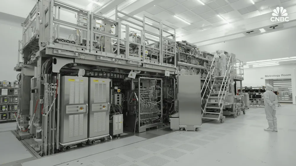
ASML CEO Christophe Fouquet reportedly told the Financial Times that it will take 10 to 15 years for AI to transform society and industry in a major way.
The comment, reported in late September, draws attention not only to today's massive investment in GPUs but also to how semiconductor manufacturing itself will change beyond it. ASML already plans to increase production of its existing lithography systems and has outlined when it expects major customers to adopt next-generation technology.
However, building more lithography systems is not the same as being able to mass-produce more complex chips at lower cost. The question is how long-term AI demand can be turned into real production capacity at chip fabs.
Optical components shape how far ASML can scale up
In its 2025 annual report, ASML explains that the number of lithography systems it can produce is limited by the production capacity of Carl Zeiss SMT, its key supplier. ASML sources critical optical components, such as lenses and mirrors, solely from that company.
Even if ASML expands its own assembly plants, the number of finished systems will not rise unless the supply of optical components keeps pace.
EUV (extreme ultraviolet) lithography systems use light to transfer extremely fine circuit patterns onto wafers. The optics used must draw those patterns with great accuracy while remaining reliable enough for repeated use in volume production.
Working with companies that have such advanced specialist expertise is one of ASML's strengths. But when demand surges, it is not only ASML that must expand capacity; its component suppliers must do so at the same time. Having the technology to build the systems is a different matter from being able to deliver the number the market demands.
Moves to increase output are already taking concrete shape.
In its July 15 earnings call, ASML said it expects to secure capacity to ship about 65 conventional Low NA EUV systems in 2026.
The company plans to raise that capacity by about 30% in 2027 and is considering a further expansion of about 30% in 2028. The 2028 figure, however, is not a confirmed production plan at this point.
AI also needs more than compute chips.
ASML says customers are expanding capacity in both leading-edge logic and DRAM, and it plans to increase capacity not only for EUV but also for immersion DUV (deep ultraviolet) lithography systems.
In DRAM, some steps that once required multiple patterning passes are being replaced with single-exposure EUV, while immersion DUV continues to be used. The arrival of new lithography technology does not make existing tools obsolete all at once.
Producing systems and delivering them to customers is also not the end of the process.
At customers' fabs, delivered tools must be installed and brought up to a state where they can be used in volume production. In its July explanation, ASML cited not only its supply chain and manufacturing capacity but also its installation teams working at customer sites as a factor in its ability to handle higher output.
As a result, even if lithography system production capacity rises 30%, AI chip supply capacity will not necessarily rise 30% over the same period. Several steps remain, including upgrades that improve the performance of existing tools, before delivered equipment turns into actual production capacity.
Higher output and next-generation adoption run on different timelines
ASML's next-generation lithography system, High NA EUV, raises the numerical aperture (NA) of the optics from the current 0.33 to 0.55.
According to the official specifications, both the conventional and High NA systems use EUV light at a wavelength of 13.5 nm, but the resolution of the patterns they can print improves from 13 nm with the conventional system to 8 nm with High NA.
Rather than shortening the wavelength of the light itself, the technology improves the optical system to form finer patterns. The 8 nm here is the resolution of patterns the lithography tool can form; it does not refer to a manufacturing process name such as an "8nm process."
If finer patterns can be printed in a single pass, patterns that were previously formed in multiple steps may be made in fewer. Samsung and ASML also hope High NA can simplify DRAM manufacturing.
But higher tool performance alone does not mean immediate adoption in volume production.
Customers must verify, application by application, which interconnect layers can use fewer exposures and whether manufacturing costs can be reduced compared with existing processes.
ASML's increase in production of existing tools, Samsung's and TSMC's adoption of High NA, and the later shift to large-format photomasks are each moving on different timelines.
The table below summarizes the target, timing and certainty of what was announced in the July earnings call, the September 8 joint announcement with Samsung and the joint announcement with TSMC.
All are future plans or goals, and DRAM and leading-edge logic have different uses. Earlier adoption dates cannot simply be read as differences in technological capability between companies.
| Timing | Party and subject | What was announced | Certainty |
|---|---|---|---|
| 2027 | ASML Low NA EUV supply | Raise production capacity by about 30% | Plan |
| 2028 | ASML Low NA EUV supply | Raise it by a further ~30% | Under consideration |
| By 2028 | Samsung's future DRAM | Introduce High NA into volume production | Plan |
| From 2030 | TSMC's leading-edge nodes | Introduce High NA into volume production | Intention |
| By 2031 | Joint initiative led by ASML and TSMC | Set up a pilot line for 12-inch masks | Goal |
| 2033 | Same joint initiative | Have lithography systems supporting large masks ready for volume production at leading-edge nodes | Goal |
The shift to large photomasks is a separate effort from the first introduction of High NA into volume production.
ASML and TSMC have outlined a plan to first introduce High NA using the 6-inch masks now in use, and then move to larger 12-inch masks.
A photomask is the original plate used to transfer a chip's circuit pattern onto the wafer. Making it larger is intended to raise productivity and reduce constraints when stitching together multiple exposure fields.
The 2033 date, however, is a goal for reaching a state that supports volume production, not a technology that has already been achieved.
Improving chip performance is also becoming harder to achieve simply by shrinking circuits on a flat plane.
ASML's explanation of Moore's Law cites new materials and three-dimensional transistor structures, as well as the importance of advanced packaging that combines multiple chips.
Building transistors in three dimensions and stacking and connecting separately manufactured chips are distinct manufacturing technologies. High NA EUV handles the step of forming extremely fine circuit patterns, not equipment for stacking chips.
In other words, next-generation chips require more than simply increasing the number of lithography systems.
Precisely overlaying fine patterns onto complex structures, and inspecting whether they have been built as designed, become even more important. The long-term technology roadmap includes not only progress in lithography itself but also the technical maturity needed to use it in stable volume production.
AI demand lifts chips, and AI enters the manufacturing floor
In September 2025, ASML announced a €1.3 billion investment in Mistral AI, giving it a stake of about 11% on a fully diluted basis.
The long-term partnership announcement described a plan to combine ASML's knowledge of chipmaking equipment and manufacturing processes with Mistral AI's models and AI agent technology.
An equipment maker that benefits from growing AI demand is itself trying to use AI to manage the complexity of manufacturing processes.
The uses go beyond engineers asking questions of a chatbot.
According to an official explanation from June 12, ASML has used AI for optical proximity correction (OPC) for more than a decade.
OPC is a technique that predicts in advance the pattern distortions that occur during actual exposure and corrects the pattern on the photomask to cancel out their effects.
AI has mainly been used to speed up calculations, but the collaboration with Mistral AI also aims to find better correction conditions and shorten the time needed to set them up.
In January 2026, ASML completed initial validation of generative AI capabilities together with customers. This does not mean, however, that the capabilities have been deployed for practical use with all customers.
Similar thinking is applied to tuning EUV light sources and inspecting chips.
If EUV source settings can be optimized with AI, it may reduce the work of engineers testing conditions one by one.
In inspection using electron beams, AI can be used to improve image quality and to choose which locations on a wafer to examine in detail. Inspecting every location at the same level of detail takes time, so balancing inspection accuracy and throughput is a challenge.
AI is also being applied to equipment maintenance.
It supports the work of analyzing error logs and past service records to identify the cause of a failure.
ASML says that in initial tests with Mistral AI, it was able to cut error diagnosis time by more than 70% for some subsystems while maintaining diagnostic accuracy equivalent to that of engineers.
However, it has not disclosed absolute diagnosis times, the number of test cases or detailed evaluation conditions.
This is ASML's assessment of specific diagnostic tasks; it does not mean that overall lithography tool uptime or productivity across an entire fab improved by 70%.
This distinction also matters when considering the "10 to 15 years" outlook Fouquet described.
AI lifts demand for compute chips and memory, and chipmaking equipment in turn grows more sophisticated. At the same time, a loop is beginning to form in which AI helps design, tune, inspect and maintain that complex equipment.
Whether improvements from individual early tests can be reproduced reliably across an entire fab, however, is still to be verified.
Will the capacity increase planned for 2027 progress through actual tool delivery and start-up? In which of customers' manufacturing steps will High NA bring cost reductions? How far can AI-assisted maintenance shorten equipment downtime in volume production?
If such results accumulate one by one, ASML will be able to expand capacity for making AI chips while also using AI to improve the very equipment that supports that production.
What will support the long-term view that AI's impact continues for 10 or 15 years is not the forecast number of years itself, but the production capacity and technological progress that actually build up in chip fabs.