

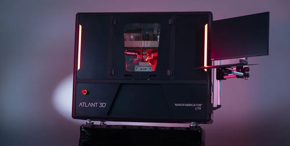
On July 16, 2026, ATLANT 3D announced that an unnamed "leading global AI hyperscaler" has ordered its NANOFABRICATOR LITE. The buyer is described as an AI-driven materials discovery lab that plans to fabricate and validate AI-generated materials, then feed the resulting experimental data back into model training. Target applications cited include semiconductors and advanced packaging, as well as photonics, energy, and quantum technology.
This news is not the invention of a new deposition principle. ATLANT 3D's Atomic Layer Additive Manufacturing (ALAM) and Direct Atomic Layer Processing (DALP) were already documented in a 2023 peer-reviewed paper covering ZnO deposition and its application to thin-film transistors. What has changed is that the seller has disclosed that a major company scaling up computational materials candidates is now installing equipment for the physical sample-fabrication step.
What can be confirmed from the announcement is limited to the order itself. The buyer's name and price are undisclosed, and delivery timing and equipment configuration have not been revealed. How it connects to measurement systems and how much the experimental cycle will shrink also remain unknown. There is no basis yet to conclude that AI materials discovery has become autonomous or is directly linked to mass production.
The Order Addresses the Gap Between AI Prediction and Physical Validation
In materials discovery, even when a model proposes candidates, those candidates must be synthesized, formed into thin films or interfaces, and measured for structure and electrical properties before the resulting data can be fed back into training. As the number of proposed candidates grows, the experimental pipeline tends to become the bottleneck. NANOFABRICATOR LITE aims to enable fabrication of samples with different conditions on the same substrate, allowing comparison of differences in materials, film thickness, and stacking order.
The sample fabrication referred to here serves a different purpose than creating wiring patterns for advanced logic chips. It is a process for preparing samples—in the early stages of thin-film materials, interfaces, and devices—to identify which combinations are worth measuring. If the round trip from an AI presenting computational candidates to receiving physical results can be shortened, both model improvement and experimental condition selection can accelerate.
The possibility that physical experimentation becomes the rate-limiting step is also evident in results from A-Lab, a separately developed automated materials discovery system. According to a report published in Nature, A-Lab synthesized 36 of 57 candidate inorganic powder compounds over 17 days, a 63% success rate. Causes of failure included reaction kinetics and precursor volatility, as well as amorphization and computational errors. While NANOFABRICATOR differs from A-Lab in both target materials and equipment, the stage of converting predicted candidates into physical reality involves constraints that computation alone cannot eliminate.
Therefore, the metric for evaluating this order should not be the number of candidates but the cycle time from sample fabrication to obtaining measurement results. Whether the same conditions yield the same results, and whether differences in conditions can be distinguished through measurement, also matter. At this point, with no announcement from the customer side, these figures cannot be confirmed.
Micro-Nozzles Separate Reactions and Deposit Thin Films Exactly Where Needed
Rather than flowing two reactive gases in sequence over time, DALP/ALAM separates them spatially within a micro-nozzle. By moving the substrate beneath the nozzle, the process can deposit thin films at specified locations while repeating self-terminating surface reactions. Direct patterning without a mask is a defining feature of this method.
Conventional atomic layer deposition (ALD) flows precursor A, purges, then flows precursor B and purges again—repeating this cycle over time to uniformly cover a large area. DALP instead determines the deposition location through the relative motion of a localized reactive-gas head and the substrate. This makes it possible to arrange patterns of different film thicknesses or materials side by side on the same substrate, producing the samples needed for comparative testing.
The 2023 paper in Small confirmed self-terminating growth of ZnO at 200–250°C, reporting 0.9 Å/cycle for ALD versus 1.1 Å/pass for ALAM. It also demonstrated line widths of 400 µm with a standard nozzle and 100 µm and 50 µm with advanced nozzles, and fabricated thin-film transistors from ALAM-deposited ZnO.
Combining atomic-layer reaction control with direct patterning allows fine-grained variation of material fabrication conditions. However, the work of selecting precursors and temperatures for each material chemistry and verifying the reaction window remains. Even if an AI proposes a material name, that output is not automatically converted into a deposition recipe or device performance.
Don't Conflate LITE's Line-Width Specs With Research-Grade Achievements
The term "atomic precision" should not be used to equate self-terminating growth in the film-thickness direction with lateral pattern formation. Controlling a film layer by layer and drawing lines laterally are distinct capabilities, and line-width figures cannot be read directly as film-thickness precision.
According to ATLANT 3D's official Solutions page, the LITE unit now on order supports up to two materials, a 400 µm line width, samples up to 100 mm, and a deposition speed of up to 200 mm/s. Meanwhile, the company's official homepage includes a card listing LITE's line width as 100 µm. Public information does not clarify which configuration this refers to, or whether the discrepancy reflects different page update times. The 100 µm and 50 µm figures from the advanced nozzles shown in the research paper must also be treated separately from the publicly listed specifications of the commercial device.
The Solutions page lists 25 µm as under development and 1 µm as a long-term goal—these are not currently achieved values. Furthermore, the 200 mm/s maximum refers to stage or drawing speed, not the throughput for a completed sample, which depends on required film thickness and number of scanning passes. Processing time also varies by material chemistry and temperature.
Since this operates at a completely different scale than the few-nanometer-level patterning handled by EUV lithography, it is not appropriate to view NANOFABRICATOR as a substitute for EUV. The direction this equipment is headed is materials/interface exploration and device prototyping. The value lies not in lateral resolution but in producing groups of samples under varied conditions and comparing measurement results.
The label "world's first nanofabricator" is a term used by ATLANT 3D or in media coverage. There is no confirmable information indicating that an independent body conducted a cross-comparison of microfabrication equipment and certified it as a world first. The technically verifiable characteristic is that the device handles localized ALD reactions and direct patterning within a single system.
Practical Value Hinges on Undisclosed KPIs and the Path to Mass Production
ATLANT 3D's announcement positions the device's use case as rapid fabrication/validation of AI-generated materials and generation of experimental data. However, the customer's name and price remain undisclosed, and neither the delivery date nor the operational start date is known. There has been no confirmation from the customer side. Even once the equipment is installed, the scope of experimental automation will also depend on measurement, sample transport, and data processing systems outside the deposition tool itself.
In practice, the work of selecting precursors, finding reaction windows, and controlling contamination continues. Interface evaluation is also essential. It remains undisclosed how the tool will integrate with measurement systems or whether the resulting data will have the reproducibility needed for use in subsequent model training. Without these conditions in place, the round trip between AI candidate generation and physical validation cannot close.
Lab-scale demonstration and mass-production application need to be evaluated on separate axes. For the former, the focus is on the cycle time from sample fabrication to measurement, whether results are reproducible under identical conditions, and whether the measurement system can be linked with data processing. For the latter, the question is whether a specific chemical system can be incorporated into a production process and whether the conditions for process integration and technology transfer to mass production can be met.
What NANOFABRICATOR handles is the portion of this cycle involving localized deposition of thin films to create samples. A separate mechanism is needed to automatically transport samples for structural and electrical measurement and to record results—including failures—under defined conditions. Even with fast drawing speeds, if measurement wait times or recipe adjustments are lengthy, the overall lab cycle will not shrink.
The first evidence for gauging the significance of this order will be the experimental cycle time and reproducibility reported in the customer's operational disclosures. Whether mass production is achievable, meanwhile, cannot be judged without separately confirming the conditions for process integration and technology transfer.