

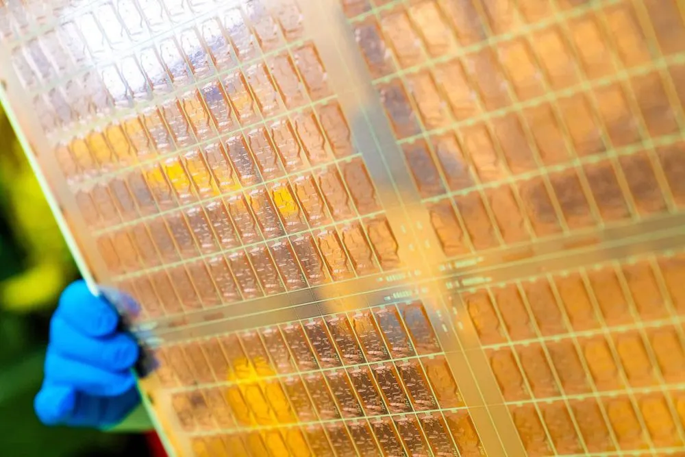
At an investor briefing on September 22, 2026, BOE revealed that it has produced 24-layer semiconductor glass substrates larger than 100×100mm and is advancing verification with customers. Having completed internal reliability testing, the company has also begun evaluations in which CPUs and GPUs are mounted on the substrates and run in servers. BOE's goal is to have the conditions in place to make a mass-production investment decision by the first half of 2027, or the first quarter if possible. As Samsung Electro-Mechanics and Dongwoo Fine-Chem's joint venture, SKC's Absolics, and LG Innotek all move toward commercialization, the years each company cites carry different meanings—ranging from investment decisions to the buildup of supply capacity.
Testing 24-Layer Substrates in Customers' Servers
According to BOE, its glass substrate pilot line can now handle the entire process end-to-end—from hole drilling through copper plating and the stacking of wiring layers to back-end processing. Chairman Chen Yanshun explained that the company is handing 24-layer products to customers for verification. This is an effort to combine substrates made through this integrated process with customers' chips for testing.
However, even after testing of the substrate alone is complete, its behavior once an actual chip is mounted must be verified separately. Xu Xiaoguang of BOE explained that work remains to verify electrical connections and overall reliability through the process of bonding and encapsulating customers' chips. Chairman Chen also said the company has begun work to build substrates carrying CPUs and GPUs into servers and run them. Moving to mass production requires that the substrate work within the systems customers actually use.
Another challenge is yield—the proportion of products meeting required quality standards. Xu said yield has improved since July, but work continues to raise it to the level needed to justify investment in mass-production equipment. The company has not disclosed specific figures. He added that how much production capacity to build and which equipment to combine also depend on this improvement.
For this reason, the first-half-2027 target BOE has set out should be read as a milestone toward a mass-production investment decision, not as a launch date. Chairman Chen cited order volumes from customers, yield, and technical requirements as the conditions involved. BOE has withheld disclosure of investment amounts and production capacity, distinguishing this stage from one where a mass-production start date has been committed to.
Lining Up Each Company's Targets by Process Stage
Samsung Electro-Mechanics and Sumitomo Chemical's Dongwoo Fine-Chem have agreed to establish a joint venture called GlaSSEM (tentative name) to commercialize glass-core substrates. Under the plan Sumitomo Chemical presented on July 2, the venture is to be established within 2026, subject to necessary approvals, with a target of building out supply capacity by the second half of fiscal 2027. The companies plan to expand supply capacity in stages after that.
At SKC, evaluation stages differ by product. According to a September 4 announcement, Absolics' embedded-type product has completed preliminary evaluation on prototypes from its Georgia plant in the U.S. and has entered reliability testing. Meanwhile, the non-embedded type is being prepared to move into PoC (proof-of-concept) by the end of 2026. SKC also announced the same day that it had approved a cash injection of roughly 281 billion won into Absolics, saying it would raise yield and quality in step with customer verification and build out a full-scale mass-production system.
Lining up each company's disclosures while keeping track of which process stage each refers to changes how the target years should be read.
| Company / Business | Disclosed Milestone / Plan | Meaning of Target Timing |
|---|---|---|
| BOE | Customer verification of 24-layer substrates; began server evaluation with CPUs and GPUs mounted | Aiming to have conditions for a mass-production investment decision in place by H1 2027, or Q1 if possible |
| Samsung Electro-Mechanics / Dongwoo Fine-Chem | Planning to establish a joint venture for glass-core substrates | Targeting buildout of supply capacity by H2 FY2027 |
| SKC / Absolics | Embedded type in reliability testing; non-embedded type preparing to enter PoC | Non-embedded type targeting PoC entry by end of 2026 |
| LG Innotek | Accelerating glass substrate technology development | Targeting mass production in 2028 |
BOE's investment decision, the joint venture's supply-capacity buildout, SKC's product evaluations, and LG's mass-production target all refer to different process stages. The table draws on BOE's September 22 briefing, Sumitomo Chemical's July 2 announcement, SKC's September 4 announcement, and LG Innotek's September 9 announcement to extract the process stage and timeframe each company is addressing. None of these should be treated as a confirmed achievement of a target date, and ranking companies' progress toward mass production based solely on the years in the table would misread the actual situation.
There is one date in LG Innotek's announcement that particularly deserves distinction. The 2027 mass-production target the company is aiming for applies to high-value-added FC-BGA for AI training and inference. FC-BGA is a type of package substrate that connects semiconductor chips to mainboards; the same announcement sets the mass-production target for glass substrates at 2028. The fact that both were showcased at the same exhibition does not mean 2027 can be substituted as the mass-production timing for glass substrates.
Glass That Enables Larger Substrates, and the Processing That Determines Mass Production
Glass-core substrates use glass for the core layer that forms the foundation inside a package substrate. Sumitomo Chemical explains that glass's rigidity, dimensional stability, and low warpage and thermal expansion make it well suited to large packages and high-density wiring. LG Innotek likewise cited the benefit of suppressing substrate warpage and circuit deformation by replacing the core layer with glass. As integration density in AI-related semiconductors increases, substrates that carry and connect chips are increasingly required to achieve both larger size and higher wiring density at once.
In manufacturing, through-holes called TGVs are drilled into the glass, metal is deposited, and wiring layers are stacked on top. What BOE describes as its integrated process is precisely this chain—from hole drilling and copper plating through ABF-based lamination to back-end processing. The figure of 24 layers shows that a multilayer substrate could be produced, but it does not indicate the proportion that can be repeatedly manufactured at the same quality.
Indeed, Xu cited the stress placed on glass as layers multiply, and the handling of debris generated during hole drilling, as manufacturing bottlenecks. He said that cleanliness in controlling fine particulate contamination also affects yield. BOE describes its thin-film and interface-processing experience accumulated in display manufacturing as a strength, but that assessment is the company's own. Translating manufacturing experience into the quality customers demand requires both the system-level evaluation described above and process improvements aimed at mass production.
The combination of Samsung Electro-Mechanics and Dongwoo Fine-Chem is also instructive when considering the manufacturing challenges that come with a material change. According to Sumitomo Chemical, Dongwoo Fine-Chem has technology for handling thin glass and experience operating automated equipment for large-area glass. Samsung Electro-Mechanics' strength lies in the design and manufacturing technology for highly multilayered, high-density wiring and large packages, including experience serving leading-edge semiconductor makers. The joint venture aims to combine the ability to process glass stably with the ability to finish it as a semiconductor package.
The Next Milestones: Orders and Yield
Following the conditions BOE has laid out for its investment decision, commercialization will hinge not just on the 24-layer specification but on whether the volumes customers need can be produced at stable quality. Even as server-based verification proceeds, it remains difficult to determine what scale of equipment to prepare until order volumes and yield reach levels that justify investment. Technical evaluation and equipment investment are linked in this respect.
SKC, too, describes the progress of customer verification separately for embedded and non-embedded types. Products in reliability testing and products preparing to enter PoC have different next milestones to clear. Rather than summarizing a company as being "close to mass production," it is easier to gauge the distance to commercialization by tracking which product has completed which evaluation.
Toward BOE's target of the first half of 2027, the test will be whether customer orders and yield meet conditions sufficient for an investment decision. If BOE then proceeds to mass-production investment, its current work testing 24-layer substrates will shift into a phase of building the supply capacity from which customers can continuously procure.