

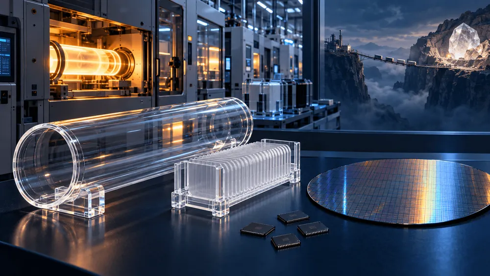
In China's semiconductor materials supply chain, a quiet but consequential advance has emerged in the localization of a basic material that fundamentally governs manufacturing yield. On September 14, 2026, TrendForce reported that Jiangsu Pacific Quartz (stock code: SH603688), a Chinese high-purity quartz materials manufacturer, has had its quartz products—made from its own proprietary high-purity quartz sand—pass product certification for use in 300mm (12-inch) wafer manufacturing at a major Chinese DRAM maker.
This series of reports illustrates how China's semiconductor ecosystem is rebuilding not just equipment and chip design domestically, but also the supply networks for extreme-environment components typified by quartz. However, it would be premature to interpret this certification as a simple case of "complete self-sufficiency in the quartz supply chain." The certified component is limited to a consumable material used in specific equipment during wafer processing. For the ultra-high-purity quartz crucibles used to produce the semiconductor substrate itself, there is still no clear path to breaking the global oligopoly held by a single mine in the United States.
What Investor Disclosures Reveal About the Gap Between Certification and Mass Shipment
The origin of this development traces back to a statement Jiangsu Pacific Quartz made on its investor dialogue platform, reported by the Chinese financial media outlet JRJ on September 2, 2026. The company explained that its semiconductor furnace tube product series, made from its own high-purity quartz sand, had passed product certification at a domestic Chinese IDM (integrated device manufacturer) with large-scale DRAM mass production capacity.
Regarding the specific identity of this customer, TP Huang, an analyst on the podcast "China Tech Talk," suggested via Tom's Hardware that it is likely ChangXin Memory Technologies (CXMT), China's largest DRAM manufacturer. However, neither Jiangsu Pacific Quartz nor TrendForce has officially disclosed the customer's name.
At the same time, Jiangsu Pacific Quartz added an important caveat to temper the market's overheated reaction. The fact that a product has passed certification does not immediately mean that large-scale commercial supply has begun. A certain evaluation period and process adjustment time is required between passing certification, fully introducing the component into the production line, and finally achieving mass shipment at scale. The company urged investors to make objective judgments based on formal disclosure documents for any material corporate information.
On the semiconductor fab floor, there exists a deep gap between qualifying a new material and actually switching procurement to it. This is especially true in DRAM manufacturing, where process geometries continue to shrink and even minute compositional variations in components carry the risk of catastrophically reducing per-wafer yield. While this announcement demonstrates that "domestically produced materials can meet the technical requirements of leading-edge fabs," it does not mean that every consumable on the production line has been immediately replaced with domestic alternatives.
5N-Grade Furnace Tubes for Heat Treatment, and a Track Record Supplying Lam and TEL
The certified component is used in the "diffusion" process, where 300mm silicon wafers are processed into chips. In other words, it refers to a consumable material used inside front-end semiconductor manufacturing equipment, after the silicon wafer substrate itself has already been completed.
In semiconductor manufacturing processes—particularly high-temperature thermal treatments such as impurity thermal diffusion and chemical vapor deposition (CVD)—quartz equipment such as furnace tubes and wafer boats, which house and protect the wafer, are indispensable. Furnace tubes generally require high-purity fused quartz in the 4N5 to 5N class, meaning silicon dioxide () with a purity of approximately 99.995% to 99.999%.
This purity control is directly tied to semiconductor device reliability. If even trace amounts of electrically active impurities or mobile ions—such as sodium, potassium, iron, or copper—are released from within the quartz at high temperatures, they can diffuse into the crystal lattice of the heated silicon wafer. This causes shifts in transistor threshold voltage, increased junction leakage current, and ultimately a collapse in final chip yield. Certification of furnace tube materials reflects a rigorous verification process by which fabs confirm that leaching of these trace impurities remains below acceptable limits.
Jiangsu Pacific Quartz's technical claims carry a degree of credibility because of the company's established track record supplying foreign semiconductor equipment makers. According to Tom's Hardware, the company obtained certification as a high-purity quartz component supplier from Lam Research and Tokyo Electron (TEL) between 2019 and 2020, and has since supplied diffusion tubes for low-pressure CVD (LPCVD), wafer boats, quartz ingots, quartz plates, and high-purity quartz tubes.
Furthermore, according to the company's Q3 2025 earnings presentation materials disclosed on October 30, 2025, its diffusion furnace tube materials made from its own high-purity quartz sand had already completed 12-inch process evaluation testing and passed certification at a major domestic Chinese memory wafer manufacturer. In this light, the current DRAM certification is not a sudden breakthrough, but an extension of a verification process that has been building since the previous year.
That said, as Tom's Hardware points out, there is no evidence confirming that all quartz consumables installed in Lam Research or Tokyo Electron equipment operating in Chinese fabs have been switched to Jiangsu Pacific Quartz products. Foreign equipment makers maintain their own global component procurement networks based on independent quality standards. What this advance represents is the establishment of one localized supply chain option—spanning from high-purity sand refinement to furnace tube component molding to installation in DRAM fab process chambers.
Jiangsu Pacific Quartz's 2026 interim report (disclosed August 22, 2026) states that its high-purity quartz materials, made from its own sand, have passed certification at multiple leading semiconductor companies both domestically and internationally. As of its Q3 2025 earnings presentation, the company's semiconductor-related business accounted for nearly 50% of total revenue, reflecting a rapid shift from solar panel components toward higher-value-added semiconductor components.
Spruce Pine's Monopoly and the Limits of Crystal-Pulling Crucibles
Behind this progress in furnace tube certification, a thick wall remains further upstream in the semiconductor materials supply chain—one that China has yet to scale. That wall is the quartz crucible raw material problem, used to pull single-crystal silicon ingots.
To manufacture semiconductor-grade silicon wafers, ultra-high-purity polysilicon must be melted using the Czochralski (CZ) method to grow massive single-crystal ingots. The vessel that directly holds this molten silicon, heated to over 1,400 degrees Celsius, is the quartz crucible. Because the crucible's inner wall is in direct contact with molten silicon, it is subject to even stricter purity standards than furnace tubes. Generally, purity exceeding 99.999% (5N) is required, and tolerances for individual harmful impurity concentrations are pushed to extreme limits.
If even microscopic bubbles or trace impurities leach from the crucible's inner surface, dislocation defects form in the growing single-crystal silicon, rendering the entire wafer unusable. As Tom's Hardware notes, the high-purity quartz manufactured by Jiangsu Pacific Quartz is not currently suitable for crucible applications requiring the 9N to 11N purity (99.9999999% to 99.999999999%) demanded for growing semiconductor-grade silicon crystals.
The number of locations on Earth capable of stably supplying natural high-purity quartz sand suitable for crystal-pulling crucibles at commercial scale is extremely limited. Two companies dominate the bulk of this market: Belgium's Sibelco, which holds mining rights in Spruce Pine, North Carolina, and Norway-based The Quartz Corp (TQC). Russia's Russian Quartz also has some production capacity, but on a limited scale.
According to a report by Sina Tech, Sibelco and The Quartz Corp together effectively control over 90% of the global high-end high-purity quartz sand market. The disruption to global semiconductor supply chains when Hurricane Helene temporarily halted mining operations at Spruce Pine in autumn 2024 remains a vivid memory. The geological scarcity of natural quartz sand is not a problem that can be easily solved through policy-driven investment or reverse engineering alone.
| Application Category | Required Purity/Specifications | Current State of Certification and Production | Main Suppliers/Origin |
|---|---|---|---|
| Crucibles for single-crystal silicon pulling | Above 5N (>99.999% ), extremely low limits on trace elements | Established commercial supply system at industrial scale | Sibelco, The Quartz Corp (ore from US Spruce Pine mine; reportedly over 90% market share per Sina Tech) |
| Front-end semiconductor equipment components (furnace tubes, etc.) | 4N5–5N grade (approx. 99.995%–99.999% ) | Passed certification for 300mm production at a major Chinese DRAM maker (mass shipment still in preparation stage) | Jiangsu Pacific Quartz (using its own quartz sand as raw material; based on JRJ report and company investor disclosures) |
| Hydrothermally synthesized quartz (next-generation material) | 5N7 (99.9997% ), yield over 85% | Completed pilot-scale process verification (large-scale industrial mass production not yet established) | Research team at Wuhan University of Technology (per Jimu News report, cited by TrendForce) |
As shown above, quartz applications in semiconductor manufacturing are far from uniform. Even as localization succeeds for components used inside front-end equipment, the choke point of raw material crucibles supporting upstream wafer production itself remains firmly in the grip of American mining regions.
Hydrothermal Synthesis Shows 5N7 Potential, But Mass Production Remains Distant
To overcome the vulnerability of dependence on natural ore, another avenue being explored within China is synthetic quartz technology—chemically manufacturing quartz.
According to a report by Hubei-based media outlet Jimu News, cited by TrendForce, a research team at Wuhan University of Technology has completed pilot-scale verification of a synthetic quartz manufacturing process using hydrothermal synthesis. This method reportedly can stably produce high-purity quartz material reaching 5N7 (99.9997% purity) with a yield exceeding 85%.
According to the reported data, the key impurity levels of this synthetic material meet the strict specifications required for advanced IC packaging substrates and optical fiber preforms. Hydrothermal synthesis is a technique that dissolves and recrystallizes silica raw material in a high-temperature, high-pressure aqueous solution environment, potentially opening a path to high purity that is not bound by the crystal structure or origin of natural ore.
However, a gap still remains between successful laboratory or pilot-line verification and economically viable industrial-scale mass production. The process of artificially synthesizing high-purity quartz requires enormous power consumption and specialized high-temperature, high-pressure reactors, and manufacturing costs per unit volume tend to spike compared to refining natural sand. The Jimu News report itself notes that most synthetic quartz projects within China have not yet reached the stage of achieving low-cost, large-scale industrial production.
Industry players are not overlooking this challenge either. According to Jiangsu Pacific Quartz's 2026 interim report, the company began construction in the first half of 2026, through a wholly owned subsidiary, of a synthetic quartz materials project with an annual production capacity of 450 tons. The aim is to capture ultra-high-purity demand in the advanced semiconductor sector and complement the physical limitations of natural quartz.
The same report also mentions that dedicated high-purity quartz materials for electronic glass cloth (Q-cloth), used in high-frequency substrates requiring low dielectric loss, have already entered small-batch supply. Efforts are proceeding in parallel to expand the company's portfolio beyond front-end semiconductor consumables into quartz applications for advanced packaging and communications infrastructure.
China's Expanding Memory Market, and the Verification Challenges That Remain
Behind Jiangsu Pacific Quartz's progress lies China's rapidly expanding domestic semiconductor manufacturing capacity, developing under geopolitical constraints.
The company's 2026 interim report analyzes that major domestic Chinese memory semiconductor manufacturers have entered their largest-ever equipment expansion cycle starting in the first half of 2026. With US export control regulations cutting off access to cutting-edge EUV lithography equipment, Chinese memory companies are racing to improve yields and expand production capacity using existing immersion DUV lithography technology and proprietary multi-patterning processes. This fab expansion rush is generating strong demand for upstream manufacturing equipment, raw materials, and consumable components.
On the memory market front, TrendForce reported separately that CXMT has launched mass production processes for next-generation mobile memory LPDDR6, reaching maximum transfer speeds of 12,800Mbps. As Chinese manufacturers drive an oversupply in commodity DRAM while simultaneously advancing toward in-house production of high-density, high-speed memory, the frequency and volume of quartz furnace tube replacements consumed within fabs is set to increase at an accelerating pace.
At the same time, the market's optimism calls for measured risk management. Jiangsu Pacific Quartz's interim report references forecasts such as the WSTS (World Semiconductor Trade Statistics) projection that the global semiconductor market will reach $1.5 trillion in 2026, a roughly 90% year-over-year increase (though the baseline market size for this comparison is not shown in the publicly available materials confirmed), and SEMI's (Semiconductor Equipment and Materials International) forecast that global semiconductor capital expenditure will reach $165.9 billion in 2026. Even so, the report remains vigilant about the industry's inherent cyclical volatility, sharp adjustments in memory pricing, and the trajectory of increasingly stringent export controls.
There is no doubt that Jiangsu Pacific Quartz's certification of furnace tube materials for 300mm DRAM production represents a case in which China's semiconductor industry has secured one small but meaningful link in its supply chain. Gaining a domestic option for procuring components that protect wafers inside high-temperature furnaces offers the practical benefit of reducing the risk of production stoppages.
However, this advance cannot be characterized as complete self-sufficiency in semiconductor materials. Key questions remain: to what degree of yield and service life will the certified material maintain as it actually penetrates mass production lines, and when and how will alternative approaches such as synthetic quartz break through the wall of crystal-growing crucibles still dominated by Spruce Pine? China's localized battle over materials is moving into its next evaluation phase—while the harshest terrain still lies ahead.