

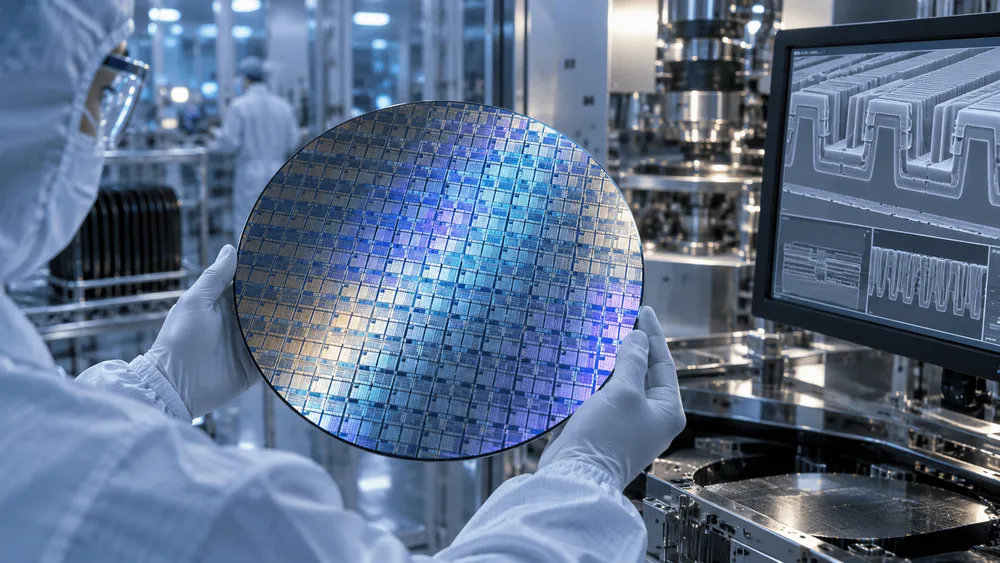
Chinese DRAM maker ChangXin Memory Technologies (CXMT) announced on September 20, 2026, the start of mass production for its fifth-generation DRAM technology platform, "G5." Two 24Gb LPDDR5X products built on G5 have also entered mass production, packaged in 496-ball and 245-ball configurations aimed at smartphones and mobile devices.
What matters most in this announcement isn't simply that LPDDR5X capacity has increased. CXMT states that by using self-aligned quadruple patterning (SAQP) to shrink the active regions of its memory array, it increased total die count per wafer by at least 50% compared to its fourth generation. This announcement signals that China's DRAM scaling technology has moved from research and development into actual mass-production processes.
However, this "50% increase" cannot simply be interpreted as a 50% boost in supply capacity. According to CXMT's own notes, the comparison refers to gross die count—before sorting for defects—normalized to 8Gb capacity. Neither yield rates nor the actual number of shippable good dies have been disclosed. To properly evaluate G5's technical progress separately from its market impact, we need to examine exactly what each figure represents.
What Does 11.95nm Actually Represent?
The eye-catching 11.95nm figure in G5 isn't a process node name describing the entire chip. What CXMT has disclosed is half the repeat pitch within the active region of the memory array—in other words, the AA half-pitch.
Simply placing this number alongside figures like "3nm" or "2nm" used for CPUs and logic semiconductors invites confusion, since these measurements target different structures and cannot be directly compared.
The technique used to create this fine periodic structure is SAQP. This process involves forming a thin film on the sidewall of a reference pattern, then using that spacer to guide formation of the next pattern—repeating the cycle multiple times.
The "quadruple" in the name doesn't mean simply exposing the same location four times. Rather, it's a method that uses self-aligned spacer formation to increase pattern density, achieving fine periodic structures that would be difficult to create with a single exposure.
Three Scaling Metrics That Define G5
The three figures CXMT disclosed—11.95nm, 45:1, and 6,762nm—each describe DRAM scaling from a different angle. In order, they represent planar pitch, capacitor aspect ratio, and core region height.
| Disclosed Metric | Target | What It Tells Us | What Remains Unknown |
|---|---|---|---|
| 11.95nm | AA half-pitch of memory array | Active regions were densified in the planar direction | Overall chip node classification, apples-to-apples comparison with competing products |
| 45:1 | Array capacitor aspect ratio | A thin, deep capacitor structure was formed | Charge capacity, retention time, improvement rate versus 4th generation |
| 6,762nm | Core region height | HKMG was introduced, fitting the core region within this height | Details of measurement scope, reduction rate versus 4th generation |
Because DRAM stores charge for each bit, simply shrinking planar dimensions alone cannot increase density. To reduce cell area while maintaining necessary storage capacity, capacitors must be formed thinner and deeper.
The 45:1 aspect ratio is one indicator of how difficult it is to form this three-dimensional structure. CXMT states this was achieved through process changes and new materials, but has not disclosed specific measured values for capacitor capacity or data retention time.
The company also states it introduced high-k metal gate (HKMG) technology for DRAM, compressing the core region height down to 6,762nm.
Furthermore, CXMT explains it built a digital twin environment that integrates design, tape-out, manufacturing, and yield management. DRAM scaling isn't purely a lithography challenge—it requires simultaneously advancing transistors, capacitors, wiring, and mass-production management together.
Note that while these three values were obtained from actual products, CXMT notes they include normal measurement variance. Additionally, since absolute values for the fourth generation weren't disclosed, generation-over-generation improvement rates cannot be calculated from the 45:1 or 6,762nm figures alone.
The "50% Increase" Doesn't Mean Supply Capacity Rose 50%
CXMT's announcement actually contains two different "50% increase" claims: per-die capacity for the 24Gb LPDDR5X product, and gross die-per-wafer count (gross DPW) normalized to 8Gb.
These two figures use different comparison baselines, and neither represents yield rates or the actual number of good dies produced.
| Subject of "50% Increase" | Comparison Baseline | What It Means | What It Doesn't Mean |
|---|---|---|---|
| Per-die capacity of 24Gb LPDDR5X | Same-category product from previous generation | Bits handled per die increased by 50% | Chip count per wafer, yield rate, memory capacity in end devices |
| G5's total die count | 4th generation, normalized to 8Gb | Using the same 8Gb baseline, pre-sorted die count arrangeable on a wafer increased by at least 50% | Yield rate, good die count, actual shipment volume, monthly production capacity |
24Gb means 24 gigabits, equivalent to 3GB in byte terms. It does not mean a 24GB memory package. To equip a device with 24GB of memory, multiple dies or multiple package configurations would be required.
The other figure, "total die count," is a metric showing how efficiently the wafer can now be utilized due to scaling.
However, even if more dies can be arranged on a wafer, if the proportion of unusable dies due to defects increases, the number of good dies won't increase at the same rate. Additional deposition and etching steps required by SAQP, along with manufacturing time and equipment utilization rates, also affect production costs.
CXMT states that G5 improves power efficiency and cost competitiveness, but the information disclosed so far doesn't allow calculation of a specific cost reduction rate.
Furthermore, it would be inappropriate to reverse-calculate from the "at least 50% increase in total die count" figure that die area shrank to exactly two-thirds of its previous size.
This is because unusable regions at wafer edges, scribe lines, and die arrangement methods or shapes haven't been disclosed.
The 8Gb-normalized figure CXMT presented is a number normalized to compare products of different capacities on the same baseline—it doesn't represent the actual die count for the 24Gb product itself.
What's Needed to Assess G5's Mass-Production Competitiveness
G5 represents clear technical progress in the sense that CXMT has actually introduced an 11.95nm AA half-pitch and 24Gb LPDDR5X into real mass-production processes.
Also worth noting: the manufacturing technology platform "G5" and product interface standards like LPDDR5X or LPDDR6 belong to separate classification systems. So the fact that G5's flagship product is LPDDR5X doesn't necessarily mean it represents an older generation of DRAM products.
On the other hand, there still isn't enough information to objectively assess CXMT's claim of "approaching world-leading mass-production DRAM."
This is because pitch and die area measured using the same definitions as competitors, along with operating speed, power consumption, data retention characteristics, and defect density, haven't been disclosed.
Monthly wafer input volume, yield rates, actual shipment volumes, and customer adoption also weren't disclosed in this announcement.
What matters next is how stably this scaled-down design can be produced as good dies.
Once customer adoption of the 24Gb product, yield rates in production lots, measured speed and power consumption values, and shipment scale spanning multiple quarters become clear, we'll be able to assess whether the increase in 8Gb-normalized total die count actually translated into real cost reductions and improved supply capacity.
The start of G5 mass production shows that CXMT has advanced to a new stage in DRAM scaling. However, determining how competitive this technology truly is in mass production compared to rival companies will require additional data on yield, performance, and actual shipments.