

Chinese DRAM maker CXMT's trial production of 8-layer HBM3 has a yield of only about 25%, South Korea's ChosunBiz reported on September 9, 2026. That is a harsh figure for China, which wants to supply high-bandwidth memory for AI domestically, but it cannot be read immediately as a "mass-production failure." A June analysis contained an estimate at a similar level, so this report alone does not show a sudden decline, and multiplying the per-process rates does not reproduce the overall figure. To judge CXMT's supply capability, we first need to confirm what this 25% means, and then look at the steps that turn DRAM into good HBM.
Rereading 25% and "80% fail" from the denominator
Citing an anonymous semiconductor equipment industry source familiar with CXMT's situation, ChosunBiz's report puts the front-end yield at about 30%, and the share of those that pass and then become good products after back-end processing at about 70%. These are not measurements published by CXMT, and the inspection conditions and the period covered are not disclosed.
Yield is the share of what is put into a process that remains as good product. So if the units that pass the front end are sent on to the next stage, the back-end 70% is not a share of the original total input. Assuming the same units pass through both stages in sequence, 30% × 70% is 21%, which does not match the roughly 25% given for the whole article.
| Source of figures | Front end | Back end (of front-end passes) | Product of the two | Overall yield cited |
|---|---|---|---|---|
| ChosunBiz, report of Sept. 9, 2026 | ~30% | ~70% | 21% | ~25% |
| SemiAnalysis, model estimate of June 23, 2026 | ~35% | ~70% | 24.5% | ~25% |
The calculated values in the table are arithmetic products of the stated rates, not a recalculation of CXMT's actual yield. Because the rounding of the approximate figures and the underlying population are unknown, we cannot determine why the discrepancy arises.
Meanwhile, SemiAnalysis's analysis of June 23 models the front end of 8-layer HBM3 at 35% and the back end at 70%. That gives 35% × 70% = 24.5%, consistent with "about 25%." However, placing an estimate from a different point in time next to an anonymous source's account does not support the conclusion that the front end worsened from 35% to 30%.
The cumulative statement "about 80% of 100 units do not become good products" and the statement "about 80% of 100 units entering final inspection fail" locate the failures in different places. Using the report's 70%, the failure rate of units that proceed to the back end is about 30%. The 80% figure should not be treated as the failure rate of final inspection alone.
Bonding gets harder as thinner DRAM is stacked higher
CXMT already lists DDR5 and other DRAM as official products. But the ability to manufacture DRAM itself is not the same as the ability to connect multiple chips vertically and finish them as HBM.
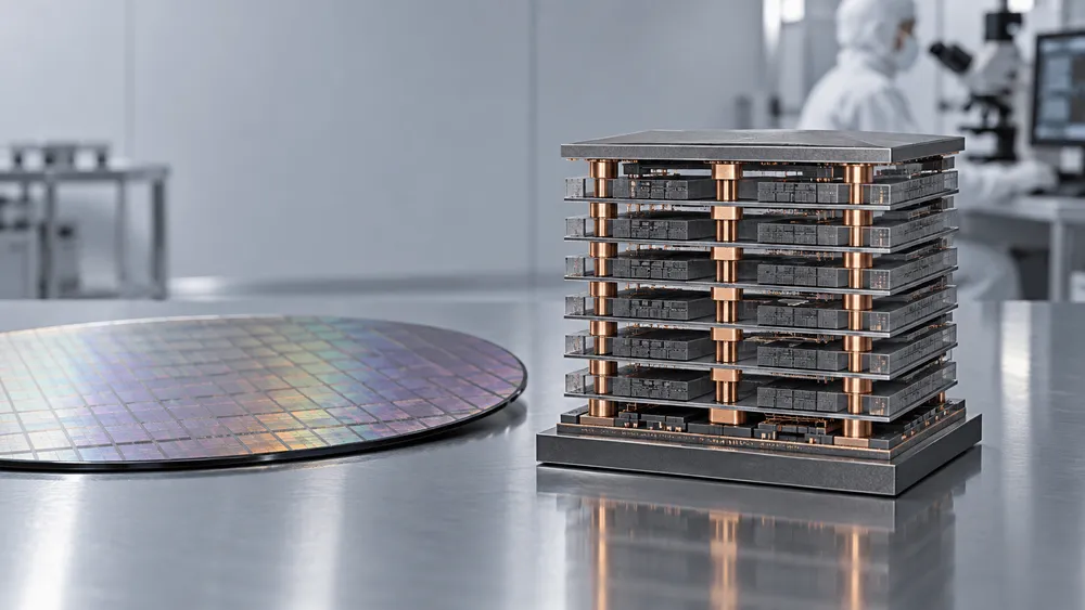
HBM stacks DRAM chips and connects them with many vertical wires. The TSV, or through-silicon via, described in SK hynix's technical explanation, is an electrode that runs vertically through a chip. At the boundaries between chips, minute contacts are joined so that signals pass through the whole stack. Even if the internal electrodes are formed, the finished product will not function unless alignment and bonding during stacking are appropriate.
Moreover, height cannot be increased freely. When SK hynix developed 12-layer HBM3 in 2023, it made each stacked DRAM 40% thinner to fit within the same height as the earlier 8-layer product. According to the development team's explanation, thinning makes chips more prone to warping, which it addressed with an improved encapsulation material and Advanced MR-MUF, a stacking and encapsulation technology.
The precision of thinning, the conditions for stacking and bonding, and the material that fills gaps and protects the chips must all work together. As the number of layers rises, so does the number of joints that must stay sound within a single finished product. The development experience of leading makers concretely shows manufacturing problems that cannot be solved just by preparing miniaturized DRAM.
That said, this is SK hynix's process. It does not mean CXMT uses the same materials or methods, or that it can improve yield in the same time. There is no basis for reducing CXMT's problem to the lack of one particular machine or a single bonding method.
Different roles for pre-stack screening and post-stack testing
A technical briefing from chip-test equipment maker Advantest in November 2023, page 16, divides HBM testing into stages before and after stacking. In the example process, DRAM dies and logic dies are each tested before stacking, and multiple tests are also performed after stacking. It is not a single gate that examines the finished product at the end.
Before stacking, the aim is first to select good chips. What Advantest defines as a known good die is an unpackaged chip judged good by testing. If defective chips are found first, the work and materials needed to stack them need not be spent.
But being good before stacking does not guarantee being good after stacking. Even in the finished state after bonding and handling, memory access and functions must be verified. Tests that screen the quality of individual chips and tests that confirm the operation of the stacked product answer different questions.
In the same material, Advantest explains that as the number of layers and the memory density increase, test time grows, and higher speeds and greater current also become challenges for test equipment. This can also affect how many units can be tested at once. Stricter testing does not by itself increase the number of good products a factory makes, and it requires time and equipment.
Given these steps, when reading CXMT's yield, the point at which defective units were found is essential. Measures to reduce front-end rejects and measures to reduce post-bonding rejects involve different processes and different data for improvement. The overall 25% alone does not let us track which one has improved.
How yield affects good-product volume and profitability
If input volume, product, and test conditions stay the same and overall yield rose from 25% to 50%, good products would double (50 ÷ 25). This is not a forecast of CXMT's improvement but a simple calculation showing the relationship between yield and supply. Even with the same input to the factory, the quantity that can be delivered to customers changes greatly.
On the other hand, it cannot be said that doubling good products would cut manufacturing cost in half. Costs arise at each process, and increasing testing or processing to raise yield adds expense. Products rejected after stacking have already consumed the processing and materials used up to that point. Even for a single unit, the cost lost differs between a defect removed at the front end and one carried through to the final stage.
For this reason, no single line can be drawn saying that above a certain yield, mass production is feasible or profitable. The assessment depends on selling prices, per-process costs, and the quantities customers need. The CXMT's HBM cost or profit and loss cannot be calculated from this report, but the relationship stands: low yield limits the supply obtainable from the same input.
For Chinese AI chip designers, this is the gap between a prototype working and being able to keep procuring the memory needed for the planned number of systems. Linking a successful prototype directly to large-scale domestic substitution requires evidence in the form of shipped good-product volumes.
Between HBM3E prototype reports and commercial HBM4 shipments
At the end of August, The Information reported small-volume production of HBM3E at CXMT. Details on production scale and test conditions are unconfirmed. This 8-layer HBM3 figure cannot be carried over to HBM3E yield.
On the competitor side, Samsung announced mass production and commercial shipment of HBM4 on February 12, 2026. By its account, HBM4 doubles the number of data input/output pins from 1,024 to 2,048, and it also addressed the accompanying power and heat challenges. In the HBM race, each new generation changes the demands on connection and packaging.
Therefore, to evaluate the gap between CXMT and the leading makers, generation and layer count must be matched, and one must distinguish whether a product is in trial production, in customer validation, or shipping commercially. Ranking a prototype yield of an older generation against the performance of a new generation's finished product with a single number will not tell us how many domestic AI systems can be built.
The US Commerce Department's BIS announced additional export controls on HBM on December 2, 2024, covering not only items of US origin but also foreign-made products that become subject to the US Export Administration Regulations under specified rules. In an environment where procurement from abroad is constrained, increasing the HBM usable domestically matters a great deal. Still, the existence of the controls alone cannot explain the cause of this low yield, nor can small-volume production be regarded as nullifying them.
The measure of CXMT's next progress is whether shipments of good products under the same product and test conditions grow and lead to continued adoption by customers. Once it gets that far, Chinese AI chip designers will be able to build the expectation of using domestic memory into actual production plans.