

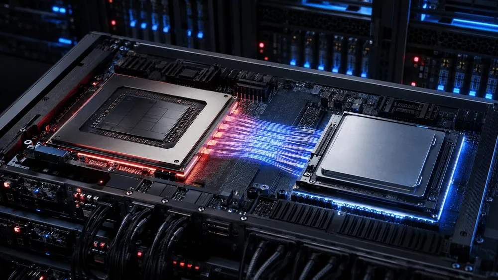
Google's TPU has evolved as a dedicated accelerator built to run AI models faster. For the next generation, there are signs that a design bringing even CPU functions inside the package itself may be under consideration. In a client note, SemiAnalysis reported market chatter suggesting that Google may be collaborating with AMD on a "TPU v10" generation project.
The note cited two reasons for this: the growing weight of CPU processing in reinforcement learning (RL), and AMD's CPU IP and advanced packaging experience. That said, neither Google nor AMD has announced a TPU v10 or any joint design effort. Whether AMD would supply CPU IP, participate in package development, or play some other role has not been disclosed.
If AMD is indeed involved, there is already material available to help interpret the rationale. Google has begun separating CPU and accelerator workloads in its current TPU lineup, and AMD has a track record of putting both on a single package. Layering the two companies' public materials together reveals the technical touchpoints this collaboration talk might be pointing to.
What SemiAnalysis Reported Remains "Market Chatter"
SemiAnalysis wrote that there is "market chatter" about Google and AMD collaborating on a TPU v10 project. According to a publicly shared excerpt of the note, Google and its customers are seeking TPUs that integrate CPU cores into the same package for reinforcement learning purposes, and AMD's CPU IP could be attractive for this. AMD's advanced packaging experience was also mentioned as a reason it could be a candidate.
However, this wording does not indicate that a contract has been signed or a design has been adopted. There is no information indicating progress on development—from tape-out to manufacturing contracts to order volumes. Delivery timelines, commercial customers, and deal value have not been confirmed either. "TPU v10" itself is not a product name Google has announced; it is a term used by SemiAnalysis.
What Google has officially announced are its eighth-generation TPUs, TPU 8t and TPU 8i. Announced at Google Cloud Next in April 2026, the 8t is designed for pre-training, while the 8i is designed for sampling, inference, and post-training. This latest speculation should be treated as concerning a design beyond these announced generations.
AMD's name surfacing also does not mean Google is handing over the entire TPU to an outside party. At this stage, all that can be confirmed is that SemiAnalysis raised CPU IP and packaging as possibilities.
Reinforcement Learning Is Bringing CPU and TPU Closer, But the Workloads Aren't the Same
Google states that it designed TPU 8i for inference and reinforcement learning. The 8i comes with 384MB of on-chip SRAM, 288GB of HBM, and 19.2Tb/s of ICI bandwidth, and Google says that under its test conditions, it cut on-chip collective communication latency by up to five times compared to the previous generation and improved inference cost-performance by 80%. Beyond the computation needed to run a model, the process of running inference repeatedly has been factored into the product design.
At the same time, Google explicitly states that CPU services complement TPUs and GPUs. It assigns complex logic, tool calls, and feedback loops surrounding the model to the CPU, citing specific examples such as RL reward computation, agent orchestration, and nested visualization. In reinforcement learning, model computation—which suits tensor operations—coexists with general-purpose processing that handles conditional branching and external tools. The claim that CPU processing is increasing does not mean that RL training as a whole is becoming CPU-centric.
The way things are currently connected also differs from a design that places the CPU inside the TPU package. Google's technical documentation for TPU 8t/8i shows a "CPU header" housing an Arm-based Google Axion CPU present in both systems, described as providing headroom for data preprocessing and orchestration.
In other words, Google has already combined CPUs and TPUs as a system. What SemiAnalysis describes as an on-package CPU would be a proposal to close that distance even further. However, the CPU header in TPU 8 is not described as integrating CPU cores into the same package as the TPU. The publicly disclosed design and a design that may be under consideration for the next generation should not be conflated.
The CPU business relationship between Google Cloud and AMD itself is not new. Google states that it adopted AMD's and Intel's latest x86 processors for its fourth-generation Compute Engine VMs, optimized for a wide range of reinforcement learning tasks including reward computation. However, this is a supply relationship for cloud CPUs, and it does not corroborate a joint TPU design.
MI300A's Track Record and the Scope AMD Might Be Able to Handle
With the MI300A, AMD has integrated 24 Zen 4 x86 CPU cores, 228 CDNA 3 GPU compute units, and 128GB of unified HBM3 into a single package. Peak memory bandwidth reaches 5.3TB/s. This confirms that AMD has actually designed data center products that place a CPU and a large-scale accelerator close together with shared memory.
This experience is not grounds for assuming AMD's MI300A design would be repurposed for Google's TPU. TPU is Google's proprietary accelerator, while MI300A is an AMD Instinct product. The CPU architecture, core count, and memory configuration cannot be inferred from this market chatter. How chiplets would be connected, and which processes would be placed on the same package, also remain unknown.
Even so, there is concrete background supporting AMD as a candidate. In November 2025, the company indicated a strategy to expand its Embedded business into semi-custom silicon and pursue co-development programs with strategic customers. It stated that it would leverage a broad range of IP and advanced packaging, but made no mention of Google or TPU. What is confirmed is only that AMD has a policy of expanding semi-custom projects and a track record of products that integrate heterogeneous computation onto a single package.
The Room Left by the Long-Term Contract with Broadcom
Google has another publicly disclosed partner in the next-generation TPU story. According to an 8-K that Broadcom filed with the U.S. Securities and Exchange Commission in April 2026, the two companies signed a long-term contract under which Broadcom will develop and supply future generations of custom TPUs. Under a separate supply assurance agreement, Broadcom will supply networking and other components for next-generation AI racks through as late as 2031.
The same disclosure also indicated that Broadcom, Google, and Anthropic are expanding their collaboration, with plans for Anthropic to gain access to roughly 3.5GW of next-generation TPU-based compute resources starting in 2027. However, this is contingent on Anthropic's continued commercial success. While this shows that Google's TPU supply plans are already tied to large-scale compute resource procurement, it does not corroborate the scale or intended use of the market chatter concerning AMD.
Therefore, it would be premature to read the AMD collaboration speculation as a replacement for Broadcom. It is logically plausible that Broadcom continues handling TPUs and networking components while AMD is involved through CPU IP, packaging, a different product line, or a different stage of the process. Conversely, there remains a possibility that the collaboration SemiAnalysis referenced never advances to an actual product. The publicly available materials do not yet show how roles would be divided between the two companies.
The first piece of information that would update this picture is a contract announcement from either Google or AMD. Next would come clarification on whether AMD's role is CPU IP or design support, what CPU architecture would be adopted, and how the package's interconnect would be configured. Confirmation of a tape-out or launch date would follow, at which point it would become possible to distinguish whether the TPU is deepening its external CPU coordination as a system, or whether the CPU is being absorbed into the accelerator itself.