


Let's compare the design of an optical information-processing chip to building an urban transportation network. Imagine a magical technology that lets you lay down an ideal highway with no traffic jams and no accidents. However, on the blueprint, there's a constraint: to run a single road, you must reinforce both sides with thick concrete soundproof walls that occupy an area many times larger than the road itself. As a result, you can't fit more than a handful of roads into the limited urban plot (the chip area), and overall transport capacity actually ends up suffering.
For the past two decades, "topological photonics" has been anticipated as a foundational technology for next-generation photonic integrated circuits—and it has faced exactly this soundproof-wall dilemma. Now, however, a joint research team from the Hong Kong University of Science and Technology, Southeast University, and Nanjing University has developed a new waveguide architecture that prevents backscattering of light without using any thick soundproof walls at all. The technology, published in the journal Nature, uses 100% of the prepared material as a light pathway, realizing a "4-lane photonic highway" in which adjacent lanes transmit information without interfering with each other.
The Wasted-Space Dilemma of Topological Photonic Circuits
In photonic integrated circuits, which replace electrons with light as the information carrier, the greatest enemy is light scattering. If a photonic circuit contains microscopic defects, impurities, or sharp bends, propagating light reflects backward at those points, causing severe signal degradation and noise.
An elegant solution to this reflection problem, studied since the 2000s, is topological photonics, which applies the concept of topological insulators. A topological insulator is originally a material whose bulk interior is an electrical insulator, while its surface or edges alone conduct electricity in a special state. Because this conductivity is protected by the material's geometric properties, electrons can detour around minor defects on the surface and continue flowing.
When this fundamental physics concept is brought into the optical domain, the interior of the material becomes a "photonic insulator" that blocks light of a specific frequency, while light propagates only along the material's boundary. Light traveling along this boundary is protected by a geometric property called topological protection. As a result, even if there are defects along the waveguide, the light never scatters backward—it smoothly detours around obstacles and continues propagating in one direction.
While topological protection may appear flawless, it comes with a heavy price. To create the edge modes that guide light in one direction, both sides of the edge must be sandwiched between vast photonic insulating layers (cladding layers). While the edge mode itself is localized to an extremely narrow region, most of the surrounding material occupies space merely as "dead space" whose sole purpose is to block light. In conventional structures, securing a light pathway just a few micrometers wide required surrounding it with an insulating region tens of micrometers wide—meaning that the majority of the chip area (sometimes over 90%) was occupied by wasted cladding layers, a serious problem of spatial inefficiency.
Xiaohan Cui of the Hong Kong University of Science and Technology points out the issue with conventional designs: "The propagating mode is strongly localized at the interface, while most of the surrounding insulating material remains inert as cladding." The more one tries to enhance a circuit's error tolerance, the smaller the effective area actually available for routing light becomes. There existed a deep-rooted tradeoff between spatial efficiency and robustness that was not easily overcome. Overcoming this dilemma was the most critical challenge for making next-generation photonic integrated circuits a reality.
The Breakthrough: "Photonic Valley Half-Semimetal"
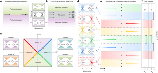
To break through the spatial-efficiency dilemma, the research team introduced a new optical state called a "photonic valley half-semimetal (PVHSM)." The team meticulously designed a structure in which cylindrical rods of the magnetic material yttrium iron garnet (YIG) are arranged in a honeycomb lattice. Within this special lattice structure, the behavior of light is strongly governed by extrema in momentum space called "valleys." By manipulating the geometric symmetry of the crystal lattice, these valleys can be used as independent information-transmission channels.
The team precisely tuned the structure to simultaneously break both time-reversal symmetry and spatial-inversion symmetry. Ordinarily, an optical waveguide transmits light in both directions, but by exploiting this symmetry breaking, they succeeded in giving the lattice a distinct dual nature. For a light valley attempting to propagate in one direction (say, rightward), the structure behaves like a gapless semimetal, acting as a waveguide that smoothly transmits the light. Yet for a light valley attempting to propagate in the opposite direction (leftward), the exact same structure stands as a topological insulator, completely blocking the light's progress. In other words, a single region becomes a "road" for light traveling in one direction and a "wall" for light traveling in the opposite direction.
A "4-Lane Photonic Highway" Where Regions Serve as Each Other's Walls
The research team skillfully combined regions with this dual nature to construct a groundbreaking architecture. They prepared four PVHSM regions, each with different properties achieved by adjusting the rod diameter and the external magnetic field, and arranged them in parallel.
When region A serves as a road that transmits rightward-propagating light, the adjacent region B acts as an impassable insulating layer for that same rightward light. Conversely, when region B transmits leftward-propagating light, region A becomes the insulating layer for that leftward light. By alternating regions with different properties, the team created a structure in which neighboring regions serve as "walls" that prevent each other's light from leaking out.
Thanks to this clever interlocking mechanism, inert cladding layers become entirely unnecessary. Every single region of the prepared material serves as a waveguide for light traveling in one direction or the other. In the experiment, the team constructed a total "4-lane photonic highway"—2 lanes for rightward propagation and 2 lanes for leftward propagation—achieving 100% space utilization. Whereas conventional designs could only fit a single pathway (1 lane) within a given chip area, the new structure successfully arranged 4 parallel lanes within the exact same spatial width. This represents an unprecedented breakthrough, suppressing the inert region of the prepared material to 0% and raising spatial utilization to 100%.
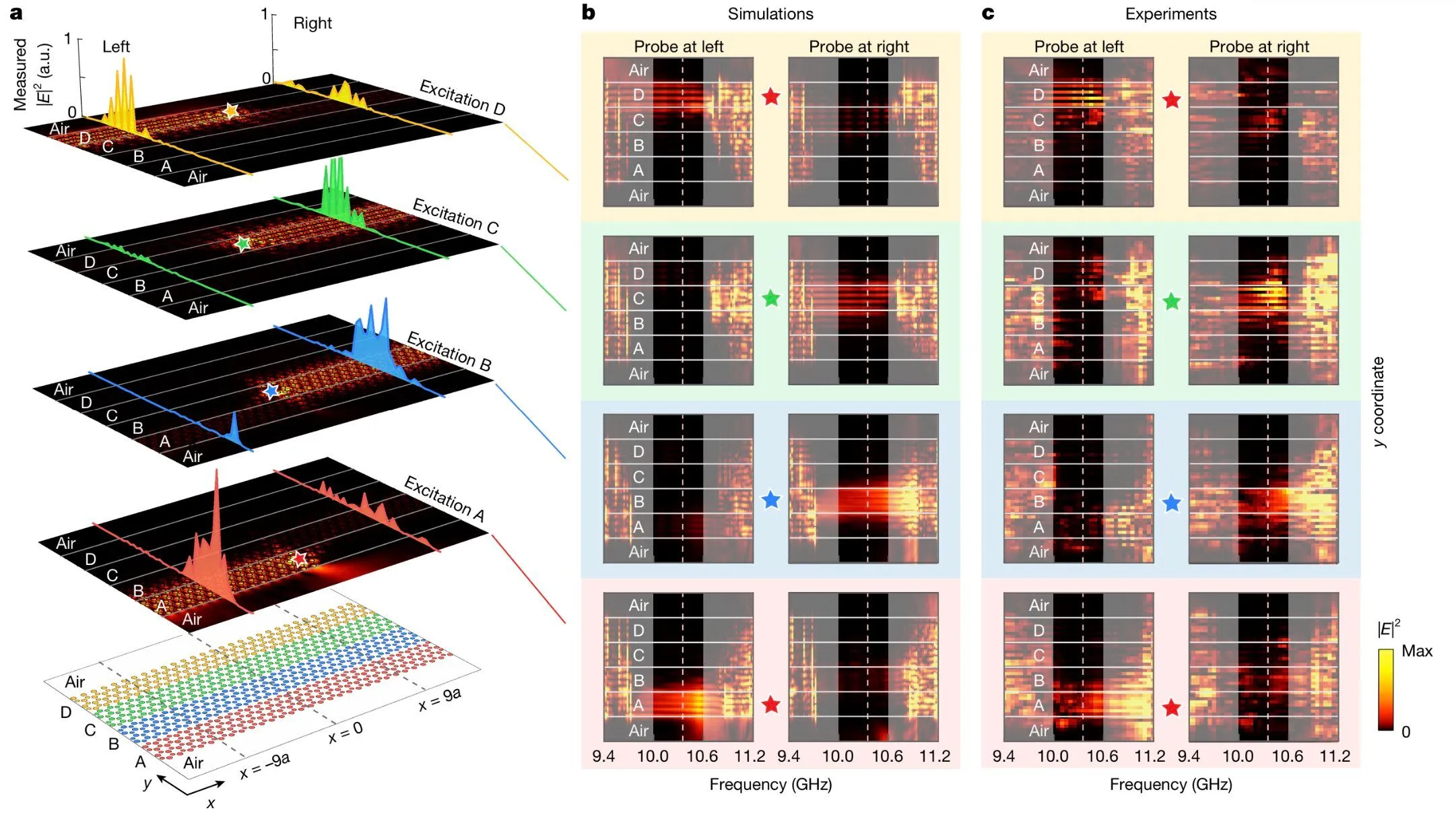
In demonstration experiments using microwaves, the photonic highway showcased the full strength of topological protection. Even when sharp bends or narrow bottlenecks were deliberately introduced into the structure, light continued propagating smoothly without backscattering. No crosstalk leaked into adjacent lanes, and signal purity was maintained. Even after eliminating the insulating layers, robustness was not compromised in the slightest.
Geometric Constraints and the Challenge of Higher Frequency Bands
This architecture—which fully leverages the benefits of topological protection while leaving no inert region whatsoever—has the potential to fundamentally transform how photonic circuits are designed. Mahmoud Jalali Mehrabad, a quantum optics researcher at the Massachusetts Institute of Technology (MIT), highly praises the significance of the paper. "Spatial efficiency has been a major problem in topological physics. This paper tackles that core problem head-on, and it's extremely important," he says, emphasizing that this achievement will have a major impact on the field as a whole.
At this stage, clear hurdles remain before practical application can be realized. This vivid demonstration was conducted in the microwave band (a few GHz), where wavelengths range from a few centimeters to millimeters. However, actual optical communications and on-chip information-processing devices standardly use light in the terahertz band (hundreds of THz), with wavelengths of a few hundred nanometers to a few micrometers. Scaling up the operating frequency roughly 100,000-fold—from the microwave band to the terahertz band—will be the biggest challenge going forward, since it requires fabricating extremely fine honeycomb structures with nanometer-scale precision.
Another physical constraint is that magnetic effects relatively weaken at higher frequency bands. The research team believes that using magnetized semiconductors such as indium antimonide should make realization in the terahertz band fully feasible. However, how to suppress the propagation losses characteristic of high frequencies while precisely managing geometric complexity remains untested. "Precisely managing geometric complexity, manufacturing tolerances, and propagation losses, while efficiently coupling with other components such as light sources and detectors, will be the major experimental challenge going forward," Cui says, describing the outlook.
The blueprint for an ideal photonic highway with 100% space utilization has finally been presented. What awaits next is the unresolved question in materials science and nanofabrication technology of how to render this beautiful blueprint onto an actual nanoscale silicon chip. It marks the dawn of a new challenge as topological photonics moves toward true practical implementation.