

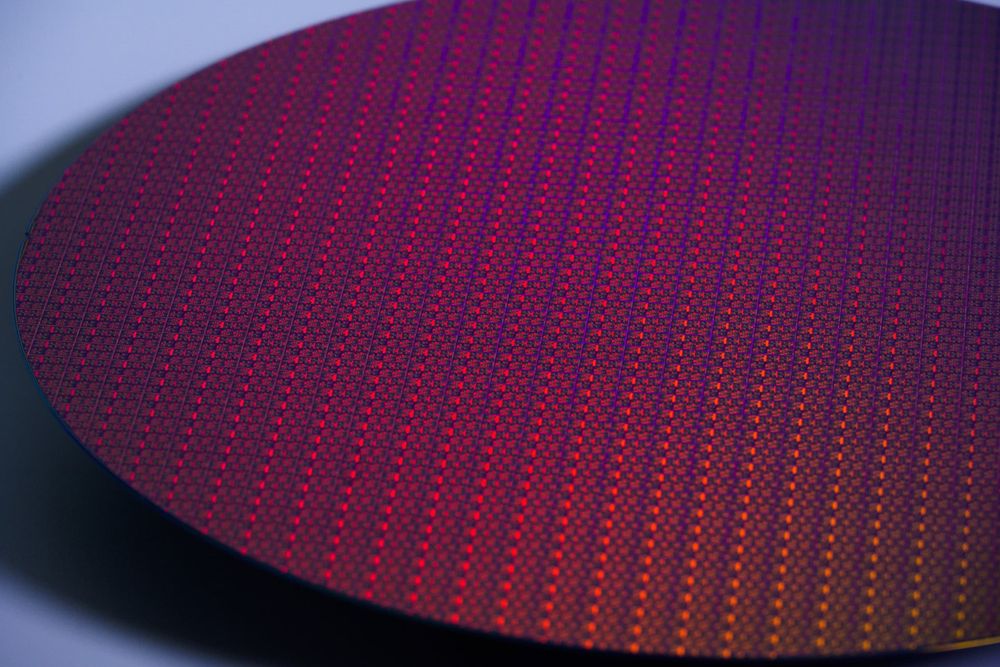
On September 15, 2026, GF Securities analyst Jeff Pu posted a mid-quarter update on X stating that the yield for Intel 18A used in Panther Lake was "still around 80%" in Q2 2026. An 80% figure would suggest that the ramp-up of this leading-edge process has progressed significantly. However, the post does not disclose the measurement conditions, and Intel itself has not disclosed absolute yield figures. Without confirming what this number is actually measuring, it cannot be extended to apply to 18A as a whole or to the good-die rate of finished CPUs.
Who Measured 80%, and What Exactly?
The 80% figure did not come from Intel's earnings materials or technical announcements—it is an analyst estimate from Pu's own X post. While the post specifies "18A (Panther Lake)" and Q2 2026, it does not indicate which SKU was being measured or how figures from Fab 52 in Arizona and the development line in Oregon were aggregated. The wafer start timing, number of dies inspected, and evaluation period all remain unknown.
Reports from outlets like TechPowerUp also reference an earlier 85% figure from a separate July report, as well as a 65% figure for Q2. But there is no evidence that these three numbers were measured at the same fab, for the same SKU, or at the same inspection stage. Plotting them as a timeline showing 15-point improvement from 65% to 80% would force numbers with different definitions into a single series. Any such comparison should be treated with caution.
In principle, improved yield increases the number of sellable dies per wafer, which should lower the per-die manufacturing cost. However, Panther Lake's actual cost cannot be calculated from the 80% figure alone. This would require wafer input costs, die area, SKU-specific binning ratios, plus the losses incurred during packaging and final testing. Fab 52's utilization rate and High-NA equipment throughput also factor in. Even with a high yield rate, if volume remains low and cannot absorb equipment costs, profitability may not improve significantly.
The 80% figure can be traced back to Pu's own X post. However, the fact that it is his own post is separate from whether it represents an official value verified by Intel. The post itself provides no measurement definition or sample size, giving no basis for treating it as an Intel-confirmed figure.
The Denominator Changes Between Compute Tiles and Finished CPUs
In semiconductor manufacturing, yield values differ depending on what counts as a "good" unit. Functional yield—whether the circuit works—is distinct from parametric yield, which checks whether voltage, frequency, and power consumption fall within spec. Dies that function can be binned into different SKUs (higher or lower tier) based on their characteristics. Process pass-through rates during manufacturing, the ratio of sellable dies, and post-packaging finished-product yield are all different metrics that don't necessarily align.
This distinction matters especially for Panther Lake. Even if a compute tile made on Intel 18A passes as a good die, it still needs to go through the process of being combined and connected with other tiles and tested as a finished CPU. Conversely, a compute tile that fails to reach the highest clock speed might still be sellable as a lower-tier SKU. Whether the 80% figure refers to the functional yield of 18A compute tiles or the post-binning sellable rate changes what it actually means for cost.
Die area also affects the probability of encountering defects. A figure obtained for a Panther Lake tile of a certain size cannot be transferred to larger server dies or 18A-P products. Even under the same process name, product yield depends on design and die area.
Three Pieces of Yield Information Are Not the Same Number
When laid side by side, public information indicating 18A's maturity falls into three distinct categories: the analyst's 80% is an absolute value; ASML's announcement is a relative comparison between exposure paths; and Intel's earnings reports indicate production status and improvement direction.
| Information | Subject | Denominator/Comparison Basis | Confidence Level |
|---|---|---|---|
| 80% | 18A for Panther Lake, estimated by Pu | Undisclosed | Analyst estimate |
| Equivalent to NXE | High-NA path for specific dual-qualified 18A layer in Oregon | Relative comparison to conventional NXE path | ASML official |
| Increased output | Intel's factory operations | High factory yield and improved cycle time | Intel official |
The analyst's 80% is an absolute figure but with an undisclosed definition; ASML's NXE-equivalent claim is a defined relative comparison; and Intel's high-volume production and increased output figures are disclosures of status and direction. These three cannot be substituted for one another. What ASML announced on July 15, 2026, was the fact that a portion of Panther Lake production had moved High-NA EUV into high-volume manufacturing, and that a specific 18A layer had been dual-qualified with a yield equivalent to the conventional NXE path. This demonstrates that the High-NA path does not disrupt mass production, but it does not reveal what percentage either path actually achieved.
Intel's Q2 earnings report points in a consistent direction. CFO Dave Zinsner explained that high factory yields and shortened cycle times led to output exceeding expectations. However, this statement concerns the factory network as a whole—there is no breakdown specific to 18A. While the official materials don't directly verify the 80% figure, they also don't contradict a picture of improving production.
From Shipping 3 SKUs to High-Volume Production
The change in Intel 18A is reflected more in the state of the product than in any single yield rate. Intel shipped 3 SKUs of Core Ultra Series 3 by the end of 2025 and officially launched them at CES in January 2026, stating that adoption would extend to over 200 notebook PC designs. In its Q2 10-Q filing, Intel stated that it has been running 18A products in high-volume manufacturing since early 2026.
The ramp-up hasn't been without bumps. As of Q1, Intel still described 18A as being in an early stage, and projected that an increasing share of 18A in the product mix would pressure Q2 gross margins. With a new process, equipment depreciation and low initial yields get baked into product costs. Even as shipment volumes increase, matching the profitability of a mature process isn't guaranteed right away.
Still, supply volume increased in Q2, and high-volume manufacturing using High-NA began for part of Panther Lake. The official materials confirm a shift from the stage of merely being able to ship products to a stage of scaling volume while using multiple exposure paths. This shift in status is the backdrop against which the 80% estimate has drawn attention.
The Next Test: 18A-P and Larger Dies
Intel 18A-P entered risk production in June 2026. Intel claims that, compared to 18A, it offers 9% higher performance at the same power, or 18% lower power at the same performance. However, these are performance and power measurements based on things like routed circuits—not yield figures. Design rule compatibility also does not guarantee the same yield rate as 18A.
For 18A to establish itself as a manufacturing platform beyond a single notebook PC compute tile, it needs to be reproduced in more demanding products. Intel introduced Xeon 6+ as its first 18A server product. Going forward, the question is whether 18A-P can move into high-volume manufacturing and demonstrate a stable characteristic distribution even on larger server dies. If products from external foundry customers are added to the mix, it would also enable evaluation independent of Intel's own designs and binning practices.
What would change this assessment is yield data that clearly specifies the fab, SKU, evaluation period, and whether it is functional or parametric yield. Once that kind of disclosure is in place, the 80% figure can move from being a headline number to becoming a comparable metric for measuring 18A's cost structure and supply capacity.