

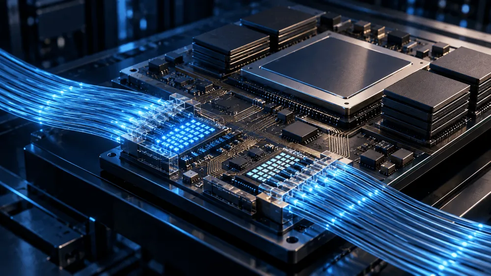
Intel is exploring a collaboration with Taiwanese display maker AUO on advanced packaging that uses Micro LEDs, Taiwan's Economic Daily News reported on September 21, 2026. The reported aims are co-packaged optics (CPO), which put optical components in the same package as compute chips, and dense chip integration. AUO has already announced work on short-range optical communication modules and glass-core substrates, and is looking to extend its display manufacturing know-how to AI. However, the two companies have not officially confirmed a partnership, and the Intel patent that the report ties in does not, on its own, show that optical communication is ready for practical use.
According to the Economic Daily News, Intel declined to comment. AUO Chairman Paul Peng has said previously that the company is co-developing advanced packaging and glass substrates with partners, but he did not name them. It is therefore too early to assume that the scope of any collaboration, a contract, or a mass-production schedule has been settled.
From making screens to short-range optical links
The optical communication technology AUO announced on August 31 targets short-range connections of up to 10 m inside AI data centers. In an announcement ahead of SEMICON Taiwan 2026 (September 2–4), the company introduced a system-level Micro LED CPO optical module developed with partners. It uses tiny LEDs as the light source for transmitting data and photodetectors to receive it.
The design relies on parallelizing many low-speed channels. Instead of pushing a few optical channels to higher speeds to increase throughput, it spreads data across many Micro LED channels. Even if each channel runs slowly, adding more paths sent at once produces a large total bandwidth. AUO says this approach reduces reliance on power-hungry signal compensation and eases the thermal burden.
This is where display experience matters. Handling large numbers of small light-emitting elements requires mass transfer, which moves them into position in bulk, and fine wiring connected to each element. Communication adds optical coupling, which feeds the emitted light into fibers. AUO says it will handle mass transfer, packaging using a redistribution layer (RDL), optical coupling, and system design. This is not about putting a screen on a CPU; it is about applying the manufacturing techniques for arranging and connecting light-emitting elements to data transmission.
Ennostar supplies the light source and Tyntek the photodetectors, combined with Corning's optical fiber technology. AUO's role is the process of making the individual components work as a single communication module. The announcement also cites applications beyond CPO, including active optical cables (AOC) with built-in optical-electrical conversion. Because implementation changes depending on where the conversion is placed, the label "Micro LED CPO" alone does not mean the technology has been chosen for any specific CPU or GPU.
What glass-core substrates and light sources each do
The glass-core substrate that AUO and Corning presented in the same announcement is a package-side technology, on which chips are mounted. It combines Corning's semiconductor glass with AUO's RDL process to support the dense wiring needed by increasingly large AI chips. Its role is separate from that of the Micro LEDs used for optical communication.
AUO cites glass's low thermal expansion, dimensional stability, and low signal loss as reasons for using it. As packages grow larger, suppressing warpage from temperature changes and holding fine connection positions become more important. The RDL is a layer that routes wiring out from terminals, while a through-glass via (TGV) is a structure that passes through the glass to connect top and bottom electrically. Even though both involve glass, a TGV is not itself a light-carrying communication path.
AUO says it is advancing TGV formation, hole metallization, and reliability verification step by step. This also shows that experience processing glass does not automatically translate into semiconductor packaging capacity. Steps remain to confirm that connections hold after fine wiring is formed and that they withstand heat and long operation. The two technologies have points of contact, but the specifications of a product combining them would have to be presented separately.
Same Micro LEDs, different roles for the patent and optical links
The US patent "IC package with micro LEDs" (US12733303), which Intel obtained on September 8, describes a structure in which a semiconductor die with Micro LEDs is at least partly embedded in a glass substrate and powered through TGVs. It was filed on September 6, 2022, so the design did not arise in response to the reported collaboration.
The uses listed in paragraph 0013 of the corresponding published application are decorative lighting, status indication for electrical testing, and lighting up text on a CPU. Intel's Micro LED patent describes lighting and display uses, and the functions and stage of confirmation shown in the materials differ from those of AUO's optical communication module.
The difference is easiest to see by lining up each document's stated use and its development or demonstration status.
| Technology / document and date | Described function / structure | Confirmed stage |
|---|---|---|
| Intel Micro LED patent (granted September 2026, application published March 2024) | Die embedded in glass and powered via TGVs; description cites lighting and status-indication uses | Structural description in a patent. Not material showing joint development with AUO or a working optical link |
| AUO Micro LED optical communication (announced August 2026) | Short-range transmission using many emitting channels, photodetectors, and optical fiber | Developed with partners; exhibition announced |
| AUO and Corning glass-core substrate (announced August 2026) | Package substrate combining semiconductor glass and RDL | In development; TGV formation, metallization, and reliability verification proceeding step by step |
| Intel OCI chiplet (announced June 2024) | Photonic circuit with integrated laser combined with an electrical IC, packaged with a CPU | Real-data transmission demonstrated; a prototype at the time of announcement |
The table sorts the patent's description and claims, AUO's announcement, and Intel's OCI announcement by use and stage of confirmation. Because the dates and approaches differ, it is not a performance comparison. Nor can the uses listed in a patent limit other possible applications or the scope of legal protection. What it shows is that a patent on mounting light-emitting elements cannot be equated with a demonstration of data transmission.
Intel itself has announced a working optical communication demonstration using a different technology. In the June 2024 OCI announcement, it integrated a silicon photonics circuit with an on-chip laser and an electrical IC, and sent real data while packaged with a CPU. The specifications were 64 channels in each direction at 32 Gbps per channel, for up to 4 Tbps bidirectional in total. These figures are not the communication performance of the Micro LED patent; they were shown at the time for the laser-based OCI prototype.
Keeping this distinction changes how the reported collaboration reads. That the two companies' technologies could be combined is one thing; that a joint product using the same light source and substrate exists is another. A patent shows accumulated technical work, but it is no substitute for connection diagrams or performance tests of a joint product.
Measuring practicality: from the light source to the whole module
AUO cites temperature stability up to 125°C and an operating life of more than 30,000 hours for its Micro LED light source. But this is the company's description of the transmit-side source, not a guarantee for the entire module including the receiver and connections. It also does not say the 30,000 hours were achieved at 125°C. Joining the temperature and lifetime figures would promise more performance than the announcement does.
The main text of the August 31 announcement gives no specific values for the module's overall bandwidth, channel count, or bit error rate. While it touts power savings, it does not say which circuits are included in the power measurement. It is therefore not yet possible to make comparisons such as how many times more efficient it is than existing laser-based approaches.
With a configuration that uses many channels, the manufacturing conditions for connecting them together and running them stably also become subject to evaluation. If it becomes clear at what yield AUO can build modules that meet the required bandwidth using its strengths in mass transfer and optical coupling, it will be easier to judge whether its manufacturing experience translates into a business advantage. This is not a claim that there is a defect now, but a condition to check when moving the approach's benefits into a mass-production product.
If a collaboration with Intel is officially announced, the first things to look at will be the light source and substrate adopted and the processes each side handles. After that, it will be worth checking the power and reliability of the whole module at the same link distance and bandwidth. Once that is shown, it will be possible to evaluate concretely how much the technology built up for displays can cut the power and heat involved in moving data in AI systems.