

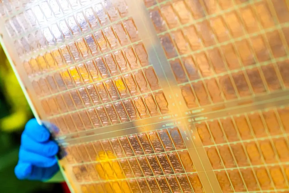
On September 8, 2026, Intel was granted a U.S. patent for embedding a semiconductor die carrying microLEDs in a glass substrate. The structure places a tiny light source inside the package, supplies it with power through wiring that passes through the glass, and extracts the light to the outside. The patent gives examples such as displaying electrical test results and making lettering glow on a CPU. But sending data with light would require a separate design that includes photodetectors and optical transmission paths. Comparing the patent with Intel's parallel microLED communication patent and its laser-based optical I/O prototype, which has already demonstrated real data transmission, shows what this invention actually aims to achieve and what would be needed to extend it to communications.
How to build a chip that glows inside glass
The U.S. patent, "IC package with micro LEDs," is registered as US 12,733,303 B2. It was filed on September 6, 2022, and published as an application on March 7, 2024; the news is that the design has now been granted as a patent. Claim 1, as listed in the U.S. Patent and Trademark Office (USPTO) gazette, specifies a configuration in which a die with attached microLEDs is at least partially embedded in a glass substrate and receives power through through-glass vias (TGVs) that contact the die.
A TGV is wiring that electrically connects the top and bottom of a substrate through holes drilled in the glass. In Figure 1 of the 2024 application publication, multiple TGVs link package substrates on both sides of the glass substrate, while other TGVs supply power and ground to the die carrying the light-emitting elements. What passes through the glass substrate is electrical wiring; the light from the LEDs is extracted to the outside through the glass. Thinking of these as two separate paths makes the aim of combining a transparent substrate with through-wiring easier to understand.
There are also several options for how the die is placed. Figure 1 shows a configuration in which part of the die is embedded in the glass with its back surface exposed, and a fully embedded example is also described. Figure 2 changes the die's orientation and connects it through surface wiring. In Figure 3, the LED-equipped die is embedded on the resin side, and a mirror reflects the light so it exits through the glass. Emission colors include red, green and blue examples, as well as a configuration in which all elements emit the same color.
Figure 4, which shows the manufacturing method, forms holes and die cavities in the glass through laser processing and etching, then creates conductive structures through electroplating and planarization. The die is then placed, and the substrates on both sides are bonded via a silicon nitride (SiN) layer. Rather than simply adding a light-emitting component to a surface, the design builds the space for the component, the power wiring and the direction of light extraction into the package manufacturing process.
Bringing decoration and electrical-test display into the package
Paragraph [0013] of the published application lists uses such as decoration, displaying electrical test results after assembly, and making lettering glow on a CPU. The description of Figure 6 also presents a configuration that lets people visually confirm that the processor is performing a particular function. The idea is to use a small light-emitting element as a display component of the semiconductor package itself.
With this design, a light source for status indication could be built into the semiconductor package. Compared with placing the indicator outside the package, the internal circuitry and the light source could potentially be connected at closer range. However, simply turning on a light is not the same as identifying the cause of a fault. Which electrical test results are displayed, and how those results are converted into light patterns, would have to be decided on the side of the test and control circuits.
The use examples in the patent alone therefore do not allow the conclusion that an autonomous fault-diagnosis system or data-center monitoring function has been completed. No product specification is shown for building LEDs into the same die as the CPU's computing circuits. What has been presented is a structure for housing a die with light-emitting elements in a package, supplying it with power and extracting its light to the outside.
What would need to be added for optical communication
Intel also holds a separate patent that includes photodetectors and optical transmission paths, "Micro-photonics parallel data transmission fabric and interconnect" (US 12,603,707 B2). It covers a mechanism in which an LED array is driven by communication data, the signals are sent into multiple optical waveguides, and photodetectors on the other side receive them. A waveguide is a component that carries light along a set path, and the document also depicts a configuration using fiber bundles.
The TGVs in the light-emitting package patent are paths for carrying power and electrical signals; the photodetectors and waveguides needed for optical communication are described in Intel's separate communications patent.
Comparing the functions shown in the public materials from the same viewpoint, the scope each design covers can be divided as follows.
| Function compared | Light-emitting package design | Parallel microLED communication design | Laser-based OCI prototype |
|---|---|---|---|
| Light source | microLEDs mounted on a die | LED array driven by communication data | On-chip laser |
| Electrical connection | Power and signal wiring through TGVs | Drive circuits and detection/amplification circuits on the receiving side | Combination of a photonic integrated circuit and an electrical IC |
| Where the light goes | Through the glass to the outside of the package | Through multiple waveguides or fiber bundles to opposing photodetectors | Through single-mode fiber to the opposite side |
| Published verification | Structure and process disclosed in the patent document | Communication configuration disclosed in the patent document | Demonstration of real data flowing between two CPUs |
The sources compared are Figures 1 to 3 of the 2024 published application for the light-emitting package, the detailed description and figures of the parallel communication patent, and the "How It Works" section of Intel's 2024 OCI announcement. The table organizes configurations with different purposes according to shared criteria: light source, electrical circuitry, transmission path and whether verification exists. It does not compare the communication performance of the three.
A package that can extract light to the outside could become one element for housing a light source used in communications. But it functions as a communication path only when the design goes on to vary that light according to data, couple it into a transmission path, and convert it back into an electrical signal on the receiving side. It cannot be confirmed from these materials whether Intel has integrated this package structure and the separate communications patent into a single product.
The idea of sharing communication across many microLEDs
The parallel communication patent presents a concept in which data is divided among many small light sources instead of pushing a small number of transmission paths to extreme speeds. The design aims to secure large overall bandwidth while keeping the operating speed of each path low.
One goal is to reduce the load of SerDes, which converts parallel signals into fast serial signals and restores them on the receiving side. The detailed description of the communications patent says that using large, high-speed SerDes increases power consumption and circuit complexity, and it presents a configuration that passes electrical signals directly to the light-source array. However, there are also examples that use small SerDes for each path. The concept is not to eliminate every conversion circuit.
On the other hand, as parallelization increases the number of light sources, it becomes harder to match the many connection paths correctly. Figure 7 onward show structures that align fiber ends with arrays of transmitting elements and photodetectors. When many thin transmission paths are used, misalignment in position or orientation could prevent light from reaching the intended photodetector.
As a countermeasure, Figure 14 and others describe a training process that uses optical signals to confirm the correspondence between paths. By checking which combinations can actually communicate, the process aims to relax the alignment precision required during manufacturing.
The receiving side also needs electrical circuits. The small current generated by a photodetector must be detected and amplified, and the influence of noise must be suppressed; on the emitting side, examples of voltage-regulation circuits for driving the LEDs are also shown. Even if an LED itself is efficient, the power consumption of the entire communication path, including drive and receiving circuits, must be evaluated separately.
The same document also assumes that LED transmission distance is shorter than that of lasers, and it proposes repeaters that convert the optical signal back into an electrical signal and then re-emit it as light. More connection points mean more loss. In evaluating parallel microLED communication, it is necessary to look not only at bandwidth and power consumption but also at how many connection points are passed through and how far the required error rate can be maintained.
Real-data demonstration and the distance to mass production
At OFC 2024, Intel announced that it had transmitted real data between two CPUs using an Optical Compute Interconnect (OCI) chiplet mounted in the same package as the CPU. The light source here is not microLEDs but a photonic integrated circuit (PIC) that includes lasers and optical amplifiers. Intel explained that it combined the PIC with an electrical IC and also measured the bit error rate during communication.
The specifications announced at the time were 64 channels in each direction at 32Gbps per channel, for a maximum bidirectional bandwidth of 4Tbps. Because 64 × 32Gbps comes to 2.048Tbps in one direction, the figure is the sum of send and receive bandwidths of roughly 2Tbps each. Mistaking it for a specification that can send 4Tbps in one direction alone would overstate the bandwidth.
Intel also gave an energy consumption figure of 5pJ per bit for this OCI. However, this is the value the company announced in 2024 for the laser-based OCI, not a measurement result for the light-emitting package or the parallel microLED communication discussed here. The company described the OCI at the time of the announcement as prototype-stage technology, and a demonstration with real data must be considered separately from shipping as a mass-produced product.
The reasons for using glass substrates cannot be explained by optical communication alone. In its 2023 announcement of glass substrates, Intel cited higher thermal and mechanical stability than organic materials and the possibility of increasing interconnect density tenfold. If dimensions are stable, fine wiring is easier to place at high density, so there are advantages for large packages centered on electrical connections as well. The tenfold figure is a possibility presented for interconnect density and does not mean CPU computing performance would increase tenfold.
To judge whether this microLED structure can move toward productization, it is necessary to verify whether the light-emitting elements and electrical connections keep operating stably through the manufacturing process after being embedded in glass, and whether light can be reliably extracted to the intended location. If it is to be used for communications, it is also essential to measure error rates on an actual link that includes the opposing photodetectors and to confirm the power consumption of the whole system, including drive and receiving circuits.
To develop a technology that builds light-emitting elements into a package into a communication path linking many CPUs and accelerators, the light source through to the receiving circuits must be made to operate as one unit and demonstrated in a structure that can be mass-produced.