

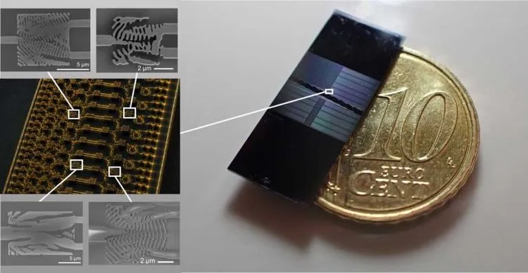
On a chip about the size of a penny, tiny structures split wavelengths of light, sort spatial modes, and reflect and confine light. Each component making up this chip has shrunk to as little as 1/500th the area compared to conventional hand-designed counterparts. This achievement comes from a research team led by Toby Bi of the Max Planck Institute for the Science of Light (MPL) and Professor Kiyoul Yang of Harvard SEAS, published in Nature Communications on May 28, 2026 (Bi et al., Nat. Commun. 17, 6943, 2026).
Photonic chips are semiconductor devices that transmit and process information using photons rather than electrons. Demand for them is growing in fields requiring high-speed, broadband data transmission—optical fiber communications, data center interconnects, LiDAR for autonomous vehicles, and quantum computing. On these chips, waveguides just a few micrometers wide carry light, while components such as wavelength demultiplexers (WDMs), spatial mode demultiplexers (MDMs), and mirrors control the light's path.
The conventional method for designing these components starts from "proven geometries" such as directional couplers or multimode interferometers, with parameters then manually tuned. This approach is time-consuming, and the range of shapes that can be explored is limited by human intuition.
The problem has been a trade-off between material choice and component size. Silicon nitride () has drawn attention as a material with extremely low optical propagation loss, well suited to generating optical frequency combs and quantum light sources. In particular, thick-film silicon nitride with a thickness of 400–800 nm achieves both low waveguide loss and strong mode confinement. However, because its refractive index contrast is lower (about 2.0) compared to silicon (refractive index about 3.5), longer interaction lengths are needed to bend or separate light, tending to make components larger. Conventional directional-coupler-type WDMs required coupling lengths of hundreds of micrometers, and coarse WDMs and MDMs sometimes reached areas on the order of square millimeters.
A design approach that works backward from the desired outcome opened up a new search space
What broke through this wall is an approach called inverse design. While conventional design starts by fixing a shape and then calculating its performance, inverse design specifies first "what you want the light to do," and a gradient-based optimization algorithm automatically searches for the nanostructure that achieves that function.
The academic roots of inverse design trace back to the late 1990s. In 1999, Cox and Dobson applied gradient methods to maximize the band gap of two-dimensional photonic crystals; in 2004, Jensen and Sigmund used topology optimization for 90-degree bends in photonic crystal waveguides. In 2015, Piggott and colleagues at Stanford University demonstrated an inverse-designed wavelength demultiplexer on a silicon substrate, and in 2017 they proposed a method for incorporating fabrication constraints directly into the optimization. A 2018 review in Nature Photonics (Molesky et al.) summarized the field as "redrawing the map of nanophotonic structures."
However, experimental demonstrations of inverse design had been limited to material platforms such as silicon, diamond, silicon carbide, and lithium niobate. A demonstration on thick-film silicon nitride had remained unachieved, since the low refractive index contrast tends to make the design region relatively large.
Bi and colleagues' team ventured into this uncharted territory. They fed the algorithm not only the optical functions required (wavelength separation, spatial mode sorting, high reflectivity) but also fabrication constraints (minimum feature size, robustness to manufacturing variation) as inputs. Professor Yang stated in a Harvard SEAS press release, "Inverse design becomes practical only when you build the realities of fabrication into the optimization itself."
Numbers from three types of components
The team designed, fabricated, and measured three types of components, comparing their performance against conventional designs.
| Component | Inverse-Design Footprint | Representative Conventional Design | Area Reduction | Key Performance |
|---|---|---|---|---|
| Wavelength Demultiplexer (WDM) | 5×5 μm² – 8×8 μm² | Directional-coupler type (coupling length hundreds of μm, area tens to hundreds of times larger) | ~50–300× | Insertion loss ~−2 dB, crosstalk below −10 dB |
| Spatial Mode Demultiplexer (MDM) | 8×8 μm² – 15×10 μm² | Phase-matching type (area on the order of mm²) | ~500× | Crosstalk −18 dB |
| Mirror (Reflector) | 11×2.8 μm² | Ring resonators or DBR structures were previously dominant | Direct comparison difficult, but high reflectivity achieved within a few-μm² footprint | Reflectivity 98.5%, finesse ~162, Q-factor ~210,000 |
The WDM separates two channels at 194/232 THz and 196/202 THz within a footprint of 5×5 μm² or 8×8 μm². The MDM sorts the fundamental mode () from the first-order higher mode () within footprints of 8×8 μm² and 15×10 μm², achieving inter-channel crosstalk of −18 dB.
The mirror's performance highlighted the low loss of thick-film silicon nitride. A micro-reflector measuring just 11×2.8 μm² achieved 98.5% reflectivity, blocking unwanted spatial modes. When a pair of mirrors was placed at both ends of a waveguide to form a Fabry-Pérot cavity, light bounced back and forth between the mirrors more than 100 times before leaking out. The free spectral range (FSR) was about 144.6 GHz and 307.6 GHz, corresponding to a finesse of about 162 and a Q-factor of about 210,000.
What shapes "beyond human intuition" signify
The shapes output by the optimization are irregular patterns of holes and ridges, bearing little resemblance to the geometries a human would intuitively sketch. Bi stated in an MPL announcement, "The structures the optimization found are ones a human would never draw."
The reason these "shapes no human would draw" work is that inverse design directly searches for solutions satisfying the wave equation. Light's interference and diffraction possess far more degrees of freedom than the symmetric structures (rings, gratings, tapers) that human intuition can grasp. The algorithm searches this space of degrees of freedom following gradient information, arriving at solutions outside the human design space.
There is also significance on the materials front. Thick-film silicon nitride is a platform well suited to nonlinear optics based on the Kerr effect and to generating quantum light sources. Del'Haye stated, "Thick-film silicon nitride underpins most of the high-performance integrated photonics we work with, but the component library has been limited to hand-designed pieces." This achievement demonstrates that compact components can be used on this material platform, opening a path toward integration into nonlinear optical circuits and quantum photonic circuits.
Remaining challenges and the next step
This research has clear boundaries. The three types of components were demonstrated individually but were not combined into a complete integrated optical circuit. On-chip interactions, cumulative loss when cascaded, and the effects of thermo-optic effects remain unverified.
What the team aims for next is integrating these components with nonlinear optical circuits to generate optical frequency combs. An optical frequency comb is an "optical ruler" made of many evenly spaced wavelengths, used in precision measurement, optical communications, and quantum technology. The high nonlinearity and low loss of thick-film silicon nitride work in favor of realizing compact comb generators.
On the manufacturing side, it has been shown that inverse-designed structures are compatible with commercial foundry processes, but data on yield and long-term reliability at mass-production scale is not yet available. Extending the design algorithm itself to more complex functions (dispersion control, polarization management, etc.) also remains a future challenge.
In electronic circuit design, Google's AlphaChip (Mirhoseini et al., Nature 594, 207–212, 2021) used deep reinforcement learning to optimize chip placement and routing, shortening design periods from weeks to hours. Inverse design in photonics optimizes a different physical layer (nanoscale electromagnetic field distributions), but shares the common structure of "AI exploring a design space outside human intuition." In both optical and electronic chips, the locus of design is shifting from humans to algorithms.