


Every modern computation is made possible by electrons racing through the interior of semiconductor chips. However, along that electron pathway lies a serious "traffic jam" that has long been overlooked.
The Physical Limit Called "Contact Resistance" That Confronts Half a Century of Conventional Wisdom
The history of semiconductor performance improvement is nothing other than the history of miniaturization—shrinking transistors as much as possible (Moore's Law). Today, leading foundries such as TSMC and Samsung are competing fiercely on process nodes pushing toward the extreme limits of 3 nanometers and even 2 nanometers. However, now that device dimensions have shrunk to the scale of just a few atoms, an issue more serious than the switching performance of the transistor itself has emerged inside chips. This is "contact resistance," which occurs at the boundary between the metal electrode and the semiconductor.
Any electronic device requires metal electrodes serving as entry and exit points in order to exchange electricity with external circuits. However, when a metal and a semiconductor—two entirely different substances—are physically joined together, an electrical barrier known as a "Schottky barrier" inevitably forms at their boundary. This is a physically unavoidable phenomenon arising from the fundamental differences in the electronic properties (work function and energy bands) of the two materials.
In conventional device fabrication processes, metal electrodes such as titanium, gold, or copper are deposited externally onto silicon or 2D semiconductors. This is akin to forcibly connecting a fully paved highway (metal) to an unpaved gravel road (semiconductor). At a boundary where there is a mismatch in material properties, the cars (electrons) traveling along it are inevitably forced to slow down, causing severe traffic congestion.
In eras when device sizes were larger, the resistance at this junction fell within the margin of error when viewed from the perspective of the entire system. However, in the latest chips where miniaturization has advanced to its limits, wiring has become extremely thin, making electron scattering more likely, while the junction area has also shrunk to a minimum. As a result, a reversal phenomenon has occurred in which the contact resistance generated at the junction with the electrode—rather than the internal resistance of the transistor itself—now dominates the overall performance of the device.
The "electrical bottleneck" that arises here wastefully dissipates as heat the energy that should be used for computation. Currently, with the rapid proliferation of generative AI, AI processors such as GPUs lined up in data centers consume astronomical amounts of power, and the problem of "dark silicon" (where heat density is too high to operate the entire chip simultaneously because heat dissipation cannot keep up) has become severe. Breaking through this thermal wall and continuing the evolution of next-generation devices required a technological breakthrough that fundamentally resolves electron traffic congestion.
A Reverse Approach: Changing Only the "Properties" Without Joining Different Materials
Traffic jams occur because dissimilar materials are forcibly connected. If so, why not simply complete both roles within a single material from the outset?
In response to this intuitive question, a joint research team led by Professor Seungbum Hong and Professor Kibum Kang of the Korea Advanced Institute of Science and Technology (KAIST), along with Professor Sung Beom Cho of Sungkyunkwan University, presented an extremely elegant solution. What they focused on was a type of transition metal dichalcogenide (TMD) called platinum diselenide ().
This is an ultra-thin material with layer thicknesses of only one to two atomic layers (less than approximately 1 nanometer), yet it possesses the unique property of being able to produce both a "semimetallic" state, which conducts electricity well like a metal, and a "semiconducting" state, which functions as a transistor, by controlling minute changes in crystal state and layer thickness. The research team skillfully exploited this property and succeeded in creating continuous semimetallic and semiconducting regions within a single film.
Rather than attaching a separate metal from the outside, this structure—which changes only the electronic structure locally while maintaining the same atomic network of a single material—is called a "monolithic (single-body) structure." To use the road analogy mentioned earlier, this is equivalent to gradually transitioning the properties of asphalt into a gravel road like a gradient, rather than forcibly cutting and pasting asphalt and gravel roads together. Because there are no seams or physical barriers between dissimilar materials, the very reason for electrons to collide and scatter at the boundary is fundamentally eliminated.
Nanoscale Evidence Confirms "Zero Traffic Jam" Electron Transport
Even a theoretically excellent structure is extremely difficult to prove functional within an actual, ultra-small device. This is because, until now, there had been a lack of technology capable of directly and precisely observing how charge moves inside a nanoscale thin film.
The research team overcame this measurement barrier by constructing their own analysis platform based on atomic force microscopy (AFM). By using a tiny probe to simultaneously scan the surface topography and electrical properties of the material at atomic-level resolution, they mapped the state of charge transport in nanometer-scale units.
The observation results vividly confirmed the prior theoretical predictions. When current flowed from the semimetallic region into the semiconducting region, none of the pathway curvature or electron stagnation that had always been observed at conventional metal-semiconductor junctions occurred; instead, the current continued to flow extremely naturally in a straight line. This was the moment when the absence of an electrical bottleneck was experimentally proven for the first time in the world through direct nanoscale observation.
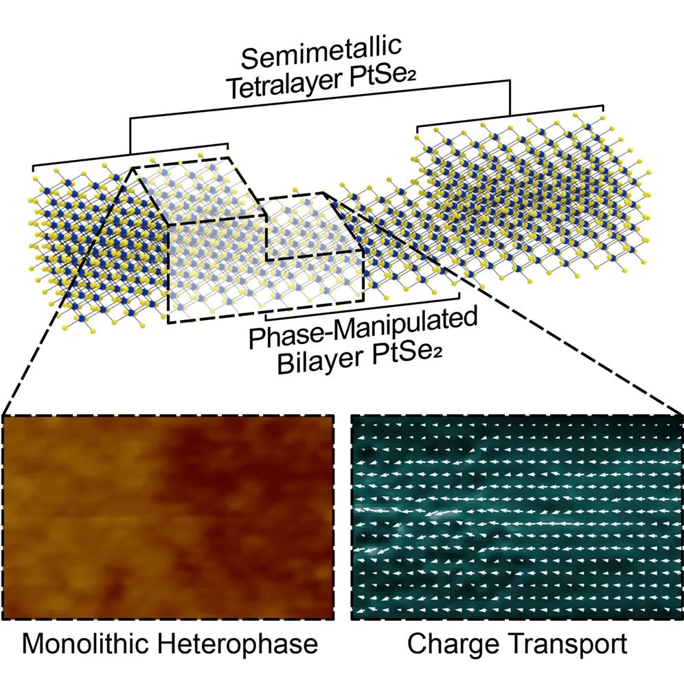
Furthermore, the team actually applied an electric field to the semiconducting region within this structure and conducted a basic operational test as a transistor. It was demonstrated that even with a monolithic interface, current on/off could be stably controlled via gate voltage. This experimental fact shows that today's discovery is not only an achievement in basic physics but also directly connects to a practical core technology for reducing contact resistance in next-generation electronic devices.
Next Hurdles Toward Room-Temperature Operation and Mass Production
This technological leap demands a fundamental paradigm shift in the architectural design of next-generation semiconductors using 2D materials. The structural differences between conventional methods and the approach of this study can be organized as shown in the table below.
| Comparison Item | Conventional (Metal Electrode Deposition) | This Study (Monolithic Structure) |
|---|---|---|
| Design Premise | Physical junction of dissimilar materials | Change in electronic properties within the same material |
| Interface Continuity | Discontinuous (barrier due to crystal structure mismatch) | Completely continuous (seamless at the atomic level) |
| Contact Resistance | Inevitably occurs, worsens further with miniaturization | Extremely low, eliminating the bottleneck |
| Cause of Power Loss | Large thermal energy dissipation at the junction | Minimized, contributing to higher efficiency |
This research (lead author: Yeongyu Kim et al.), published in the July 2026 issue of the international materials science journal Matter, serves as an important stepping stone toward evolving semiconductor manufacturing from "bonding dissimilar materials" to "transforming properties within a single material."
For AI chips that perform massive parallel computation and where thermal management is a matter of life and death, as well as ultra-low-power semiconductors required to operate for long periods on limited batteries, eliminating contact resistance translates directly into improved performance. In particular, for the semiconductor industry that is rushing to introduce 2D materials as channel materials to replace existing silicon, the value of a monolithic structure that can avoid the "contact difficulty" unique to ultra-thin materials is immeasurable.
Hurdles remain to be overcome toward practical application. First, it is necessary to establish a method for uniformly scaling up this precise monolithic structure to large-area wafers on the 300-millimeter scale used in actual semiconductor production lines. Second, durability verification is needed to determine whether the boundary state between the semimetal and semiconductor can maintain long-term stability even under the harsh thermal environment inside servers. Third, there is the horizontal expansion of how far this approach can be applied to other promising 2D materials such as molybdenum disulfide.
The fact remains unshaken that, within nanoscale space, the half-century-old convention of "joining dissimilar materials" has been cast aside, and seamless charge transport through a single material has been proven. This approach, which has opened up an electron "road without traffic jams," is certain to reliably redraw the very foundation of the architecture of next-generation devices that we will hold in our hands.