


The processors inside modern smartphones pack tens of billions of transistors into an area no larger than a thumbnail. Yet silicon, which has underpinned humanity's digital society for the past half century, now faces a physical limit imposed by the size of atoms themselves.
The End of Silicon Scaling and the Rise of Two-Dimensional Semiconductors as the Next Protagonist
The Ultimate Thinness That Suppresses Short-Channel Effects
When the distance between a transistor's electrodes (the channel length) shrinks to just a few nanometers, the "short-channel effect" becomes pronounced—the gate voltage can no longer completely shut off the current. This causes unintended leakage current even in the off state, sending the chip's overall power consumption and heat generation spiraling out of control. To prevent this, the channel itself—the pathway through which current flows—must be made as thin as possible, strengthening the gate electrode's control over the electric field.
Leading-edge semiconductor manufacturers are currently introducing GAA (Gate-All-Around) structures, in which the channel is divided into ribbon-like strips completely surrounded by the gate. However, physically thinning silicon itself any further has become extremely difficult. This is where attention has turned to (molybdenum disulfide), a two-dimensional semiconductor made of sheet-like layers of molybdenum and sulfur atoms. Using this material—just 0.7 nm thick—as a replacement channel for silicon has become a shared goal among semiconductor researchers worldwide.
The Fatal Flaw of Grain Boundaries in Powder-Based CVD
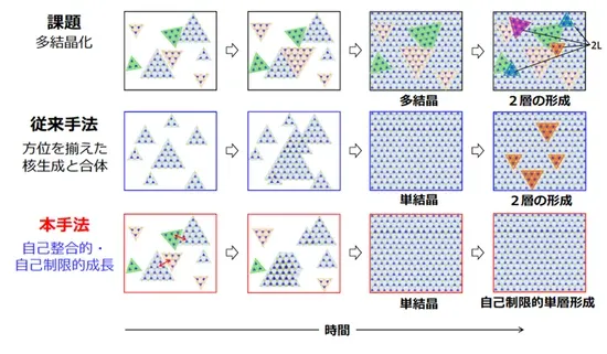
When attempting to manufacture at industrial wafer scale, a massive wall stands in the way. In the chemical vapor deposition (CVD) methods using powder precursors that have dominated research and development so far, tiny crystal grains nucleate at various points on the substrate and grow until they merge. But because their crystallographic orientations are misaligned, defects known as "grain boundaries" inevitably form.
These grain boundaries act as obstacles blocking the path of electrons. They significantly degrade electron mobility—a key performance metric for transistors—and drastically reduce chip-to-chip yield when fabricating large-scale integrated circuits. To bring next-generation logic devices to practical use, a technology capable of artificially synthesizing a "single crystal" aligned in a single orientation across an entire wafer was essential.
An Autonomous Formation Mechanism That Overturns Conventional Wisdom on Crystal Growth
The Self-Aligning Dynamics by Which Foreign Domains Spontaneously Vanish
A joint research team centered around the University of Tokyo and the National Institute for Materials Science (NIMS) has provided an answer to this grain-merging problem by adopting metal-organic chemical vapor deposition (MOCVD)—a technique with a proven track record in industry—together with a new molybdenum precursor (). MOCVD is already standard in current mass-production lines for LEDs and laser diodes, offering rigorous supply control at the molecular level.
As crystals grow on a sapphire substrate, each grain forms a periodic matching pattern with the substrate's atomic arrangement, known as a "supercell." In conventional processes, defects remain right where grains collide with one another. But in this new method, energetically unstable 60-degree antiparallel domains and rotated domains spontaneously rearrange themselves at the moment of coalescence.
This corresponds to the phenomenon of jigsaw puzzle pieces rotating into their correct orientation on their own, guided by the shape of the underlying frame at the instant they interlock. Real-space observation via differential dark-field transmission electron microscopy (Differential DF-TEM) vividly captures how this self-aligning growth mechanism weeds out mismatched domains, ultimately forming a complete single crystal with 0-degree orientation.
Discovery of a Growth Self-Termination That Stops Precisely at the First Layer
This deposition process also possesses an autonomous control mechanism in the thickness direction. Even if the deposition time is artificially extended, crystal growth halts precisely at the first layer, and no second layer forms thereafter. This is because the distinctive chemical properties of the precursor strongly suppress new nucleation on the surface of already-formed .
This self-limiting mechanism maintains a uniform, single-atom thickness across an entire 2-inch wafer. When this single-crystal film was actually transferred onto a silicon substrate to fabricate a transistor, it recorded an electron mobility of at room temperature. When the temperature is further lowered to 20 K, the mobility reaches . This behavior—mobility rising sharply at low temperatures—indicates that electrical resistance is primarily caused not by electron scattering from crystal defects, but by scattering from atomic thermal vibrations (phonons). This is solid evidence that an extremely high-purity single crystal with very few defects has been achieved.
Unmasking the True Nature of a Long-Overlooked van der Waals Interface
A Hidden Layer of Water and Dust Lurking in What Was Thought to Be a Tight Contact
Once a high-quality wafer has been achieved, the industrial imperative is naturally to use it as-is as the foundation for device fabrication. Conventionally, grown on sapphire had to undergo a "transfer" process—peeling it off using special chemicals and moving it onto a different substrate. This physical relocation step was the single greatest bottleneck preventing wafer scale-up, and it was also a breeding ground for wrinkles and contamination.
The research team skipped the transfer step entirely, building transistors by forming electrodes and a gate insulating film directly on the still on its sapphire substrate. However, the as-fabricated devices exhibited a fatal flaw: the current would not fully switch off even when a large negative voltage was applied to the gate. Quantifying the carrier concentration via Hall measurements revealed that, in the initial state with no applied voltage, a high density of excess electrons——was present within the .
The interface between sapphire and had long been regarded as an inert van der Waals interface with no chemical bonding. Interface-sensitive measurement techniques—X-ray photoelectron spectroscopy (XPS) and atomic force microscopy (AFM)—exposed the truth: hidden within what was believed to be an intimate contact was an amorphous layer, roughly 0.3 nm thick, composed of water molecules and sulfate groups ().
This situation corresponds to a structure in which a thin layer of damp, fine dust—generated by chemical reactions during manufacturing—is sandwiched between flooring (sapphire) and a carpet () laid on top of it. This trapped hydrophilic layer acted as a donor, continuously supplying static charge (electrons) to the carpet side, forcibly locking the transistor's switch into the "on" state.
Transfer-Free Dry Processing Realized by a Hydrogen-Argon Gas Treatment
To remove this hidden layer, the research team pursued a solution through a completely dry process rather than washing the wafer with liquids. The wafer was heat-treated (annealed) at 400 °C under a mixed hydrogen-argon gas atmosphere.
This heat treatment causes the water molecules bound at the interface to desorb. Simultaneously, the sulfate groups react with hydrogen to form volatile gases such as sulfur dioxide () and hydrogen sulfide (), which are then expelled to the exterior. Thermal desorption spectroscopy (TDS) data confirms that sulfur-related molecules are indeed desorbed from the interface during this process.
With the source of excess electrons cut off, the annealed device regained its intended transistor characteristics. The current now varied by orders of magnitude in response to changes in gate voltage, achieving a clearly defined off state. A method was thus established in which the entire process, from film deposition to device fabrication, is completed on a single sapphire wafer, without any transfer step or chemical treatment whatsoever.
| Comparison Item | Conventional Powder CVD + Transfer Process | This Study's MOCVD + Dry Interface Treatment |
|---|---|---|
| Single-crystallization mechanism | Relies on physical process control (grain boundaries tend to remain) | Mismatched domains spontaneously vanish through self-alignment |
| Thickness control | Requires strict management via growth time | Automatically stops at one layer due to precursor properties |
| Device fabrication process | Chemical exfoliation and transfer to another substrate required | Direct processing on the sapphire substrate (transfer-free) |
| Interface condition | Water and polymer residue contamination during transfer | Dopants completely volatilized and removed via hydrogen-argon heat treatment |
Establishing a Manufacturing Process Directly Compatible with Existing Semiconductor Mass-Production Lines
Scalability to 300 mm Wafers and Its Impact on Industry
The greatest value of this research lies in demonstrating full compatibility with the dry processes that the silicon industry has spent decades refining, in the context of circuit fabrication using 2D semiconductors. The single-layer growth-termination mechanism will serve as a powerful tool for guaranteeing uniform film thickness from center to edge when scaling up to the 300 mm-diameter wafers that future leading-edge foundries will adopt as standard.
The significance of showing a path by which giants such as TSMC and Intel—who envision sub-1nm generation chip manufacturing in their 2030s roadmaps—could refresh only the channel material while reusing the majority of their existing production lines cannot be overstated. Furthermore, this process is expected to extend beyond (an n-type semiconductor) to other transition metal dichalcogenides with p-type characteristics, such as (tungsten diselenide). With both types in hand, it becomes possible to construct truly complementary metal-oxide-semiconductor (CMOS) circuits made entirely of 2D materials.
Atomic-Level Engineering Opening the Door to the Sub-1nm Node
At the same time, mysteries remain to be solved at the microscopic scale. Cross-sectional observations via electron microscopy have confirmed that the distance between aluminum atoms on the sapphire's outermost surface and molybdenum atoms in has slightly widened after heat treatment, from 0.86 nm before treatment to 0.98 nm after. This is thought to reflect a change in interfacial interactions following the removal of impurities, but exactly how this microscopic structural change affects long-term device operational stability and reliability is a question that must be verified next.
How can an ultrathin semiconductor sheet be brought under complete control? A fundamental discovery in materials science is directly poised to reshape the future of the global semiconductor supply chain. Atomic-level engineering aimed at realizing next-generation processors has now stepped beyond the laboratory and into the full-scale phase of industrial implementation.