

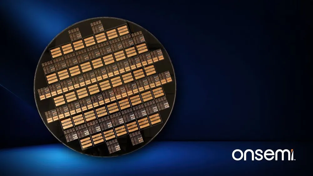
On September 16, 2026, onsemi announced the Embedded Power Platform (EPP), which uses the silicon wafer itself as the foundation of the package. The technology embeds power-switching semiconductors and their drive and control circuits in a single structure, optimizing electrical performance, heat dissipation, and mechanical design together. The company says EPP delivers 3 to 5 times the power density of conventional solutions, depending on the application, and it is targeting AI data centers and EVs. Looking at how the performance gain is achieved, the aim goes beyond making semiconductors smaller: it is to rebuild how wiring and heat removal work.
Embedding components in silicon and designing wiring and cooling together
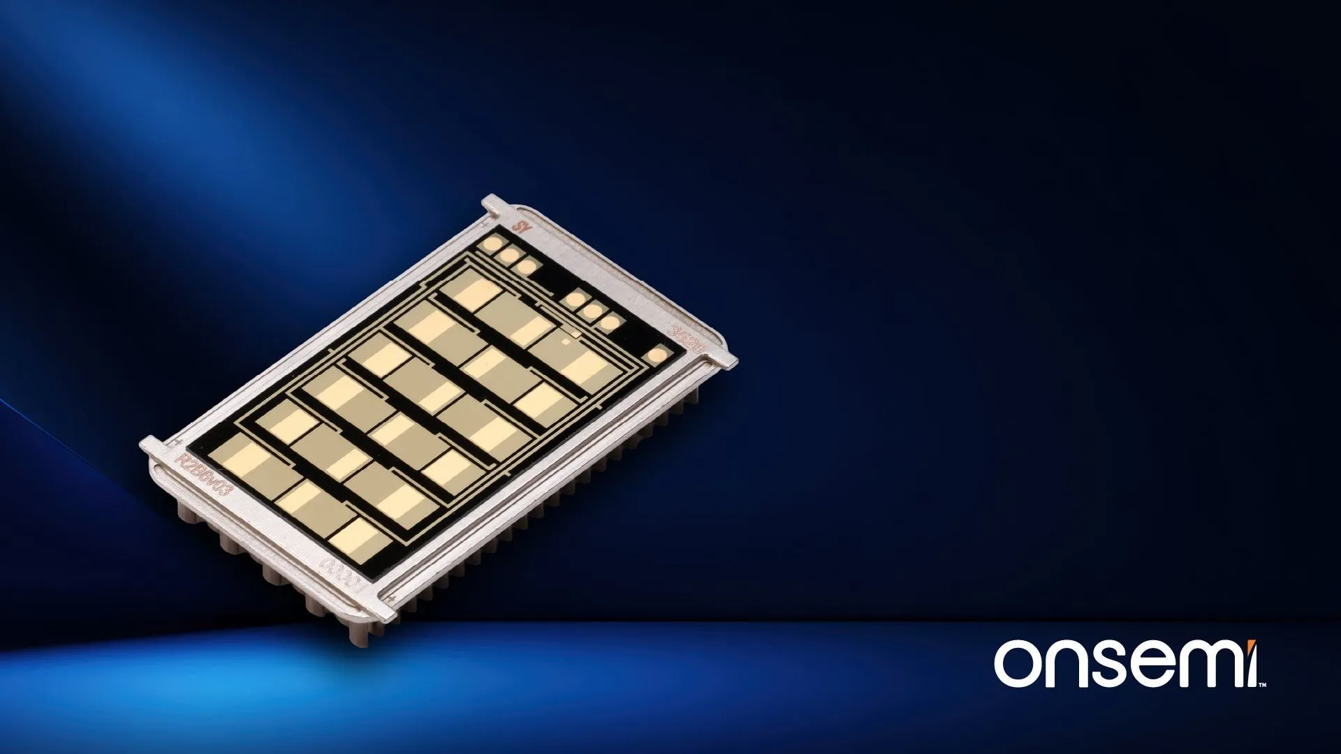
EPP embeds the transistors that switch power, along with the drivers and controllers that operate them, inside the silicon. The devices are not limited to silicon: silicon carbide (SiC) and gallium nitride (GaN) are also covered. It is a packaging approach that can combine different semiconductor technologies, not an announcement that every device is being replaced with the same material.
The company has also changed how the parts are connected. According to onsemi's technical brochure, conventional wire bonds are replaced with a redistribution layer (RDL) formed on the wafer. Moving from a structure connected by thin wires to wiring formed with precision in a semiconductor fab is meant to make the electrical paths between components shorter and easier to control.
The target of this change is parasitic inductance, which arises from wiring and similar structures. onsemi says reducing it improves device control and allows operation at higher switching frequencies. Even if a high-performance power semiconductor is chosen, its performance cannot be fully exploited if the characteristics of the connections constrain operation. By designing the devices and connections together, EPP tackles that limitation.
For heat dissipation, the design combines a silicon-based structure with heat conduction through the entire package. The technical brochure says high-voltage isolation is integrated into the same package, reducing reliance on insulating materials that conduct heat poorly. Isolation is not being eliminated; the design that separates electrical domains and the design that removes heat are handled together.
This changes the usual development sequence, in which components are chosen, then wired, and the cooling method is settled last. If a layout that favors electrical performance makes cooling difficult, the design has to be revisited late in the process. onsemi's co-design approach brings these interactions into simulation from the start, aiming to reduce rework after prototyping.
Manufacturing uses the company's standard 12-inch silicon wafer capacity. Part of the integration work that has depended on mechanical assembly moves into processes controlled in a semiconductor fab. Note, however, that what is being replaced with silicon is the structure of the power package. This does not mean printed circuit boards (PCBs) will disappear from an entire server motherboard.
Aligning the baselines behind "3–5x"
In onsemi's comparison table for investors, area-based power density is set at 1x for the leadframe/DBC substrate approach, 1.3x for PCB-embedded, and 3–5x for EPP. The structures and figures below are drawn from page 23 of the investor presentation PDF released alongside the September 16 announcement.
| Item | Leadframe/DBC substrate | PCB-embedded | EPP |
|---|---|---|---|
| Area-based power density | 1x (baseline) | 1.3x | 3–5x |
| Heat removal direction | Bottom side | Bottom side | Both sides |
The source is onsemi's comparison table. The power density row is relative to the conventional leadframe/DBC substrate approach and is not the result of independent measurement. The table does not specify the ratings of the target equipment or the cooling conditions.
In other words, this is not a figure that can be read as "5x versus PCB-embedded." It also compares the power that can be handled per unit area; it does not mean power conversion efficiency or GPU compute performance improves by the same factor. Placing the density figure next to double-sided cooling makes it easier to understand that EPP changes component placement and heat paths. Applying that improvement to a specific power supply, however, requires application-specific conditions.
For EV traction inverters, the press release cites up to 4x higher power density and 15% lower power loss than conventional approaches. The latter is a reduction in the power lost during conversion. It is not a 15-point gain in conversion efficiency, and it cannot be translated directly into a percentage increase in driving range.
For AI infrastructure, the example given is an early design of a solid-state circuit breaker, which cuts current to protect a circuit. The company says it is about 50% smaller than existing designs. However, the release contains no definition that shows whether that "size" refers to area or volume. It should not be treated as proof that the volume of an entire server power supply has been halved.
The product page also states power density of "up to 4x." It is unclear whether this was measured under the same conditions as the 3–5x, depending on application, stated in the release. The description of EPP's overall density and the individual examples for inverters and breakers should therefore be read separately.
In AI racks, the more power supplied to compute devices, the more space and cooling are needed for the equipment that converts and protects it. If EPP's miniaturization can be reproduced in real designs, it could reduce the space that power-handling equipment occupies. It is best understood as a technology that supports the race for compute-chip performance from the power delivery side.
Between shorter development and volume adoption lies evaluation
onsemi also says EPP can shorten development time to as little as four months. The means described in the technical brochure are simulation using digital twins and optimization across electrical, thermal, and mechanical domains. The aim is to reduce how often hardware must be built and tested, and to speed up design iteration.
However, the process shown on page 24 of the investor PDF does not say that customer-side evaluation can be shortened uniformly. It states that integration into systems depends on the customer and project and proceeds on the customer's own validation schedule. Even if package design and manufacturing become faster, the steps of integrating into actual vehicles or servers and confirming that requirements are met remain.
The collaboration with SUBARU illustrates this difference. According to the collaboration announcement of the same date, SUBARU will get early access to engineering samples, simulation models, and technical support, and will evaluate EPP for future electric vehicles. The initial phase focuses on technical evaluation and gaining knowledge, and no decision to adopt it in a specific production vehicle has been announced.
The explanation of supply also comes in stages. The press release says sampling will begin within 2026 for strategic customers in automotive and AI, while the investor materials say samples are already being provided. The tenses differ, but both indicate a sampling and evaluation stage with target customers, and neither means general availability or the start of installation in production vehicles.
EPP's significance lies in extending the pursuit of performance from existing power semiconductors to the design of wiring and heat dissipation. In future adoption decisions, the question will be how much size and loss can be reduced when the power and cooling conditions of each application are aligned. If customer systems confirm the effect, designers will have more options to shrink the space set aside for power supplies and protection circuits and to build denser AI equipment and electric vehicles.