

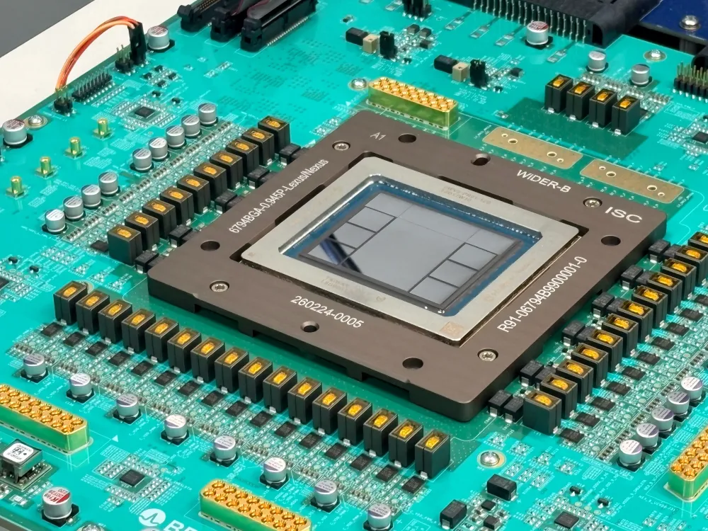
OpenAI is deepening its cooperation with Samsung Electronics on next-generation chip development. According to Reuters, Harrison Kim, head of OpenAI's Korea operations, spoke about progress in joint research and production at a press conference in Seoul on September 9, 2026. The two companies already have a partnership on memory supply for Stargate, OpenAI's AI infrastructure program, and OpenAI is also developing its own inference chip. However, Kim's remarks did not explain which components or processes Samsung will handle. To understand how far the collaboration extends, it helps to look at the technology that links memory to compute chips.
Joint research and production progress vs. an announced order
Kim described joint research and production with Samsung on the next-generation chip under development as one of the areas where cooperation has advanced most. The Reuters dispatch gave no further detail. Samsung also said it could not confirm information about customers. In other words, OpenAI spoke about progress in the cooperation, but Samsung has not announced a specific manufacturing order. Reuters also reported that OpenAI said in June that TSMC would manufacture the first-generation Jalapeño. Nothing in the latest remarks suggests that this division of labor has changed.
The companies' cooperation dates back to the letter of intent announced on October 1, 2025. Samsung Electronics set out plans to supply high-performance, power-efficient DRAM as a strategic memory partner for Stargate. The figure of up to 900,000 DRAM wafers per month cited in that announcement is OpenAI's projected memory demand. It is neither an order volume placed solely with Samsung nor an actual shipment count.
In fact, Samsung's explanation at that time already mentioned logic semiconductors, foundry capabilities, and advanced packaging in addition to memory. It cited technology for combining different types of semiconductors as a strength it could offer OpenAI. What is new this time is the statement that joint research and production on the next-generation chip has advanced. Which technology has been adopted in which product remains undisclosed.
Why memory matters for inference chips
On June 24, 2026, OpenAI and Broadcom announced Jalapeño, a custom inference chip. Inference is the process of using a trained AI model to process input and generate answers. OpenAI designs the chip around the requirements of its models and products, while Broadcom provides semiconductor implementation and networking technology. Celestica is involved in building everything from the boards to racks and systems.
What OpenAI gains from this division of labor is design freedom that is hard to get by simply fitting its models to existing semiconductors. It can decide which operations to speed up and where to keep data from waiting, based on how its AI services are actually used. Even if each component's performance improves, overall response speed will not rise if waiting time increases along the path that delivers data.
OpenAI's technical explanation of August 25 shows why, by distinguishing between input processing and answer generation. The stage that processes input in bulk is compute-intensive, whereas the stage that generates answers sequentially is more prone to memory-bandwidth limits. Communication that moves data between cores and chips also creates waiting time, so Jalapeño uses a design that controls the placement of items such as the KV cache referenced during generation, reducing data movement.
This means that for OpenAI, cooperation with a memory maker can matter not only for securing the needed volume but also for refining how data reaches the compute circuits. The specific division of design work with Samsung has not been disclosed, but this is why the technology surrounding memory is directly tied to faster inference.
The technology between memory and contract manufacturing
On February 12, 2026, Samsung announced that it had begun mass production and commercial shipments of HBM4, a high-bandwidth memory. HBM is stacked DRAM, and Samsung's HBM4 uses 4nm manufacturing technology for the logic circuitry at the base of the DRAM stack. This "logic base die" is a component on the memory side; it is not the compute chip that performs AI calculations.
For HBM4, the company says it increased data input/output pins from 1,024 to 2,048, and that its memory and foundry businesses coordinated to optimize design and manufacturing technology. A foundry is a contract semiconductor manufacturing business. Because advanced logic manufacturing capability is also used to develop memory products, a simple "memory or foundry" choice does not capture what the cooperation involves.
Samsung technologies and what has been disclosed for OpenAI (as of September 10, 2026)
| Area | What has been announced and when | What can be confirmed for OpenAI |
|---|---|---|
| Memory supply | Samsung and OpenAI announced a letter of intent for a Stargate partnership in October 2025 | Strategic memory partner. Breakdown of adoption in individual chips unknown |
| Logic inside memory | Samsung announced shipments of HBM4 using a 4nm logic base die in February 2026 | Samsung product technology. Adoption in this collaboration not disclosed |
| Compute chip–memory packaging | Samsung unveiled a concept model of vertically stacked zHBM in August 2026 | Introduction of a future technology. No adoption announced by OpenAI |
| Contract manufacturing of the compute chip itself | Outsourcing of the compute chip itself to Samsung not disclosed | The September 9 press conference did not explain the role, manufacturing process, or volume |
The table draws on Samsung's partnership announcement, its HBM4 shipment announcement, its technology presentation at FMS, and Reuters' coverage of the press conference. Being involved in manufacturing the logic inside HBM and contract-manufacturing the AI compute chip itself are separate orders. In judging the value of the collaboration, it is necessary to confirm who designs and who manufactures which components.
The division of roles to watch in the next generation
The zHBM that Samsung showed on August 5 is a concept for stacking HBM, which has traditionally sat beside the compute chip, on top of it. It aims to shorten the distance data travels and improve bandwidth and power efficiency. It also envisions building circuits tailored to customer requirements into a layer between the memory and the compute chip. However, what was displayed was a concept model, not a mass-production product for OpenAI.
Not all of Samsung's memory is at the same stage of development, either. According to the company's August explanation, HBM4 entered mass production in February, and HBM4E began shipping customer samples in May. Distinguishing shipping products, evaluation samples, and further-out concepts shows that the timing at which any of this translates into business depends on which generation a partner joins.
OpenAI plans to start deploying Jalapeño in its own compute infrastructure by the end of 2026. As of August, it says development of the second generation is under way and the third is taking shape, but it has not indicated which generations Samsung will handle. OpenAI also intends to continue deploying accelerators from other companies, such as NVIDIA, for both training and inference. It is too early to regard its custom chip development as a plan to replace existing suppliers all at once.
If the components Samsung will handle and the timing of mass production become clear, it will be possible to evaluate concretely whether the collaboration helps secure memory supply, improve data transfer, or extend to manufacturing the compute chip itself. To keep improving the response speed and power efficiency OpenAI is targeting, that division of roles will need to be implemented in next-generation products and brought into live service.