


A joint research team from JEOL, North Carolina State University, and Oak Ridge National Laboratory (ORNL) has announced that a full-size tungsten tile made with a metal 3D printer kept its shape after 74 H-mode discharges at the DIII-D fusion research device in the United States. The test was conducted in July 2026, and North Carolina State University announced the results on October 26. The tiles were installed in the divertor, a key component of a fusion reactor that removes heat and impurities from the plasma and must withstand extremely high heat loads. The result matters because it moves beyond materials testing with small samples to a demonstration with a part that was actually installed in a fusion research device. However, the temperature at the center of the plasma does not translate directly into the temperature at the surface of a component, and the test does not prove long-term durability in a power-generating fusion reactor.
Real-device test succeeds after 74 discharges and about 4 minutes of cumulative exposure
According to North Carolina State University, the research team installed the 3D-printed tungsten tiles in DIII-D's lower divertor and examined their resistance to plasma over three days. In the test, 74 discharges were performed in H-mode, a high-confinement operating regime at medium to high power, and the cumulative time the tiles were exposed to plasma reached about 4 minutes. This does not mean the tiles were exposed to plasma continuously for three days, nor that they endured a single four-minute discharge.
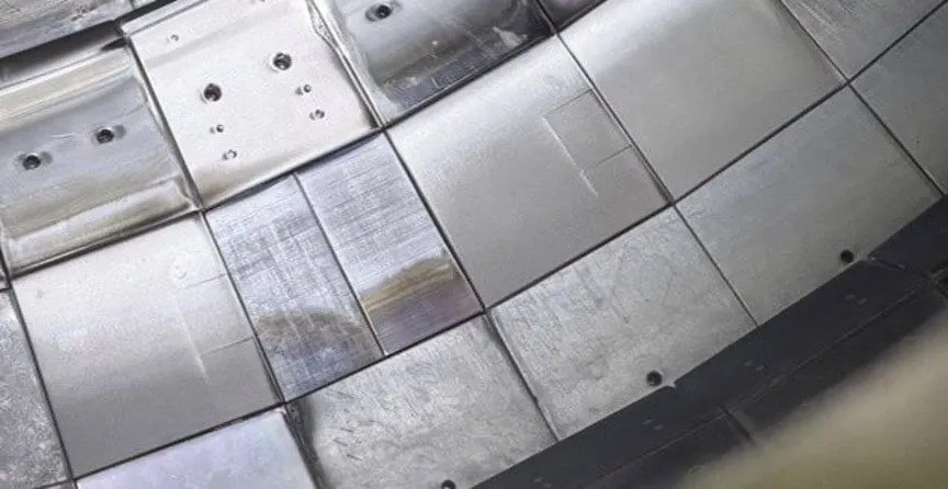
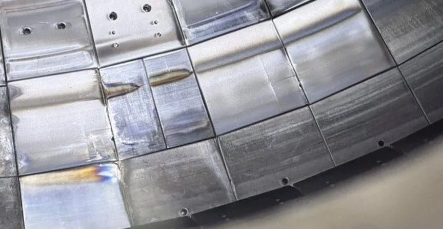
After the test, the 3D-printed tiles had maintained their shape. By contrast, the tip of an adjacent conventional tile melted because of misalignment, and some of the molten material reportedly splashed onto the 3D-printed tiles. That said, it cannot be concluded from this result that the 3D-printed parts have higher heat resistance than conventional ones. The two were not compared under identical conditions, since differences in mounting position and shape change the actual heat load each receives.
As of the announcement, the team had removed the tiles after the test and was comparing photographs and surface scan data with their pre-exposure state. After radiation safety checks, the tiles are to be taken back to the university for detailed analysis of the surface and interior. Maintaining their shape therefore does not mean there are no microcracks or internal damage in the material. The results are also based on announcements from the university and companies, and no peer-reviewed paper reporting this real-device test has been found so far.
Large tungsten components made with an electron-beam 3D printer
Tungsten has an extremely high melting point of about 3,422°C and is being studied as a leading material for components exposed to the high heat loads of fusion reactors. On the other hand, it is brittle at room temperature and difficult to machine into complex shapes. In May 2024, ORNL announced that it had manufactured tungsten parts with complex geometries using a metal 3D printer based on an electron beam. The present research develops that manufacturing technology into full-size parts and verifies it through installation in a fusion research device and plasma exposure.
The technique used is a additive manufacturing method called electron beam powder bed fusion (EB-PBF). An electron beam is directed at metal powder spread in a vacuum, melting and solidifying the required areas layer by layer to build up the target shape. According to North Carolina State University, keeping the ambient temperature during printing above 1,400°C suppresses cracking in the tungsten. This 1,400°C figure is the ambient temperature during building; it does not indicate the melting point of tungsten or the surface temperature of the tiles during plasma exposure. The distinguishing feature is the combination of locally melting the powder with the electron beam and keeping the build environment hot to suppress cracking.
ORNL explains that manufacturing with an electron beam in a vacuum helps reduce material contamination and residual stress. However, no specific figures on the purity or alloy composition of the tiles produced have been found. It therefore cannot be concluded that any particular material composition improved heat resistance or mechanical properties.
The full-size tiles were made with JEOL's metal 3D printer JAM-5200EBM. At JEOL's facility in Akishima, Japan, flat and dome-shaped tiles were prototyped several times, eventually yielding printed parts with no major defects that met dimensional requirements. North Carolina State University then handled finishing and evaluation, while ORNL contributed manufacturing funding and materials expertise.
What matters about this achievement is that the tiles were not only printed but also machined into a state ready for installation in the device. According to JEOL, the printed tiles underwent wire electrical discharge machining and multi-axis CNC grinding, removing about 250 µm of material from the plasma-facing surface. The machined tiles were then mounted on a copper alloy base. The finished tile pair measures about 136 × 143 mm and is 20 mm thick; this is the dimension of two tiles combined, not of a single tile. The manufacturing significance of this work lies in finishing material made from powder into a device-ready component with the required dimensional accuracy and surface condition, and taking it all the way to plasma testing.
How this differs from earlier tests, from small samples to full-size tiles
Evaluating this result requires understanding how it differs from tests carried out so far. In particular, the 2025 small-sample test, this full-size tile test, and the qualification test for the International Thermonuclear Experimental Reactor (ITER) each have different purposes and load conditions, so their durability cannot be compared simply.
In the 2025 DiMES test described by North Carolina State University, small button-shaped tungsten samples were exposed to plasma at a heat flux of about 20 MW/m². Short-duration peaks reportedly exceeded 35 MW/m². Heat flux is a measure of the amount of heat flowing in per unit area and is used to evaluate how much heat load a material experiences. Surface damage to the small samples in this test was reported as slight, but these heat flux values cannot be treated as the test conditions for the present full-size tiles.
Comparison of major tests related to tungsten components
| Test / timing | Subject and purpose | Published load and number of cycles | What was confirmed |
|---|---|---|---|
| 2025 DiMES test | Materials test exposing small button-shaped samples to plasma | About 20 MW/m², short-duration peaks above 35 MW/m² | Surface damage to small samples reported as slight |
| July 2026 DIII-D test | Full-size tiles installed in the lower divertor and tested | 74 H-mode discharges, about 4 minutes cumulative. Heat flux received by the tiles not confirmed | Tiles that went through printing, finishing, and installation maintained their shape |
| ITER qualification test announced September 23, 2024 | Evaluation of a test assembly for the outer vertical target | Heat loads of 5–20 MW/m² applied 6,000 times | Manufacturing process and heat removal performance qualified |
This comparison is based on North Carolina State University's test results and ITER's official announcement. However, the tests differ in the size and structure of the components, how the heat load was applied, exposure time, and cooling conditions. Comparing only the 74 discharges at DIII-D with the 6,000 cycles in the ITER test therefore cannot determine which part has the longer lifetime or greater durability.
The ITER qualification test was conducted on a test assembly for the outer vertical target developed by the National Institutes for Quantum Science and Technology (QST) and Mitsubishi Heavy Industries. In addition to the suitability of the manufacturing process, the test evaluated the ability to remove heat under high heat loads. The 3D-printed tiles have not received equivalent qualification, and the test subject and structure are different in any case. Confirming material properties in small samples, plasma exposure tests of full-size parts, and qualification tests including cooling functions should be regarded as different stages toward the practical use of fusion reactor components.
Practical use requires verification of heat removal and long-term reliability
A fusion reactor divertor must not only resist surface damage when exposed to hot plasma but also continuously remove the heat flowing into it. According to ITER's official explanation, the divertor's vertical targets are expected to see heat fluxes of 10 MW/m² in steady state and 20 MW/m² in slow transients, and the design removes heat through active water cooling. Tungsten's high melting point is an advantage in such an environment, but a material's ability to withstand high temperatures is a separate matter from whether the component as a whole can remove heat adequately. The thermal performance of the whole part, including the cooling structure, therefore needs to be confirmed for 3D-printed tiles as well.
The published information alone does not reveal the maximum surface temperature the full-size tiles reached, how much material was lost through exposure, or whether microcracks formed. For long-term use in a power-generating fusion reactor, in addition to heat removal performance including the cooling system, it will also be necessary to verify how material properties change under repeated heat loads, long-term use, and neutron irradiation. Nor is there specific information on manufacturing yield or cost for 3D printing, so it has not reached the stage where it can be judged economically superior to conventional manufacturing methods.
The achievement lies in finishing difficult-to-machine tungsten into a full-size part with a 3D printer and taking it through plasma exposure testing in a fusion research device. Detailed analysis to come is expected to reveal what changes occurred on the surface and inside tiles that kept their shape outwardly. If thermal load tests on parts with built-in cooling and long-term reliability evaluations advance further, they should yield important data for judging how far electron-beam 3D-printed tungsten components can be used in future fusion reactors.