

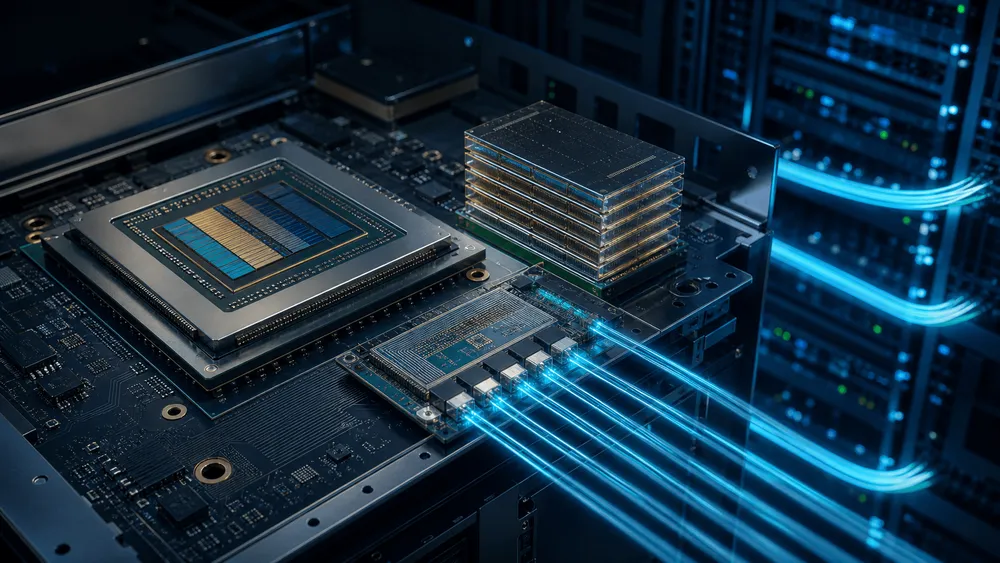
SK hynix is looking to extend optical pathways beyond HBM. The design calls for co-packaged optics (CPO)—which places processors and optical transceivers in the same package—to expand from rack-to-pod connections toward future shared memory pools. A review paper by SK hynix's Seunghoon Hong and 11 co-authors was published in Nature Electronics on August 19, 2026. As AI computing scales up, how the bandwidth problem solved near memory shifts to data movement between systems will shape the design.
A bandwidth wall beyond HBM
SK hynix states that while computing throughput typically triples every two years, interconnect bandwidth grows only about 1.4-fold over the same period. HBM stacked near accelerators widens the bandwidth reaching memory within a package. But in large-scale AI, where numerous GPUs and HBM units are bundled into racks and pods, data movement to and from distant compute resources becomes the next constraint.
The paper reviews the optical connections used to address this. Its publication type in Nature Electronics is a Review Article—not an announcement of a new CPO product or prototype chip. The paper was received on July 8, appears in volume 9, pages 853–867, and its peer review information is publicly available.
SK hynix's previous explanations centered on technologies that bring memory and logic closer together, such as advanced logic base dies for HBM4, custom HBM tailored to customer specifications, HBF, and 3D Stacked DRAM on Logic. The CPO roadmap extends that scope beyond the chip and package level to racks, pods, and even shared memory. Specifications for individual components alone can no longer fully explain the bandwidth of an entire AI system.
Shortening the electrical segment, carrying the rest optically
In CPO, the processor and optical transceiver (TRx) are placed in the same package. Traditionally, a photonic engine separate from the SoC was connected via copper wiring on a PCB; CPO instead places the TRx on an interposer near the SoC, shortening the distance traveled by high-speed electrical signals. The remaining long-distance segment is carried optically.
Copper wiring won't disappear entirely. SK hynix itself notes that copper remains cost-effective over short distances, but as speeds increase and distances grow, the burden of compensation circuitry, power consumption, and latency increases. CPO is a technology that shifts where that burden becomes heaviest by minimizing electrical wiring length.
The company's design targets for next-generation AI infrastructure are stated as more than 100 Tb/s per node, less than 1 pJ per bit, and less than 10 ns of chip-to-chip latency. However, these are all roadmap targets—not measured values achieved in SK hynix products, nor benchmarks verified in customer environments. Until an implementation combining TRx, package, and memory is demonstrated, these three metrics cannot be used to compare across products.
From 2D to 3D, eventually extending light to memory
The technical roadmap progresses through 2D implementation, 2.5D interposer-based approaches, and 3D heterogeneous integration—an order that brings optical components progressively closer to the processor as the degree of integration increases. Where the electrical and optical segments are divided within the package will also be determined according to the system's bandwidth requirements.
In the long-term vision, a photonic interposer would connect XPU pools and memory pools—extending the scope of optical connections to scenarios where multiple AI accelerators share a large-capacity memory pool. This is not yet an implemented configuration. No implementation timeline or standard has been disclosed, nor has any information been provided about the manufacturer, supported processors, or capacity.
HBM increases bandwidth within an accelerator's package, while CPO carries data outside it. By placing both on the same roadmap, the paper calls for treating memory capacity and bandwidth, packaging, and rack-to-rack connections together—as a single design consideration for where power and latency are spent.
What remains between roadmap and mass production
The publicly available abstract in Nature Electronics lists thermal management, manufacturability, and standardization as key challenges. In SK hynix's own official commentary, the research team identifies low-power photonic devices, coherence protocols, and system reliability as unresolved issues. The closer light is placed to the processor, the more the benefits of signal quality and power efficiency must be weighed alongside heat generation and assembly difficulty.
Mass production also involves yield, cost, cooling, and supply chains. TrendForce cites manufacturing yield, maintainability, standardization of optical fiber connectors, and supply of InP lasers as constraints on large-scale commercialization. Particularly in designs that bring optical components closer to the package, how to service failures and whether components can be continuously procured become conditions separate from communication performance.
Market size figures also do not imply technological achievement. TrendForce forecasts that the combined CPO and NPO market will grow from about 100 million US dollars in 2025 to over 39 billion US dollars by 2030—but this is not a forecast specific to CPO alone, nor a sales projection for SK hynix. Nothing in the company's paper indicates the start of mass production or customer adoption.
No outlook has been published suggesting CPO will fully replace copper wiring. Copper remains cost-effective over short distances, and TrendForce expects LPO, NPO, and CPO to coexist. Which connections get converted to optical will depend not only on bandwidth figures but also on maintenance methods and component supply conditions.
How far will memory companies extend into systems?
In an official article dated April 23, SK hynix explained its plan to expand from supplying standard HBM to custom HBM, adopting TSMC's advanced logic as the base die for HBM4. HBF and 3D Stacked DRAM on Logic were included in that plan as well. The policy of deepening the connection between memory and logic had already been disclosed.
The CPO paper extends that connectivity further, to optical compute interconnects. For SK hynix, this represents an extension of its existing strategy—expanding its role from a supplier of standalone memory to a technology partner co-designing customers' AI systems. However, the paper's co-authors also include researchers from the University of Virginia, Yonsei University, the University of Illinois Urbana-Champaign, Nanyang Technological University, and MIT, and Nature's page discloses Hong's employment at SK hynix as a competing interest.
What should be verified in future announcements is who will implement and adopt this roadmap, whether standards agreements are reached, and under what configuration the targets of over 100 Tb/s, under 1 pJ/bit, and under 10 ns were actually measured. Only once such details are disclosed will the vision of extending light all the way to memory move from a research roadmap to an actual option for AI infrastructure.