


On August 23, SK hynix presented a roadmap for advanced HBM packaging in the memory technology tutorial at Hot Chips 2026. The material covered three layers: the internal bonding that stacks DRAM dies, the 2.5D packaging that links HBM to compute dies side by side, and a future 3D integration that would bring the two closer together vertically. As HBM bandwidth and capacity grow, it becomes harder to build the memory first and mount it in a package afterward as a separate step. Intel's EMIB also appeared in the presentation materials, but this is not an announcement of an adoption contract. The real change is that HBM makers have made clear they are moving toward designing these three packaging layers together with their customers' compute dies.
Three Packaging Layers That Make Up HBM
The first layer is the bonding method used to stack DRAM dies vertically inside HBM. SK hynix's mass-production MR-MUF and the next-generation candidate, hybrid bonding, belong here. This process determines the spacing between dies, TSV density, and how easily heat escapes.
The second layer is the 2.5D packaging that connects finished HBM to a GPU or xPU laterally. The Hot Chips slides listed TSMC's CoWoS-S, CoWoS-R, and CoWoS-L alongside Intel's EMIB. CoWoS is an interposer-based packaging approach using silicon or RDL, while EMIB embeds small silicon bridges in an organic substrate only where needed. Each addresses a layer separate from the bonding method inside HBM.
Where the two layers meet sits the base die. It is the logic at the very bottom of HBM that binds the DRAM stack together and handles communication with the compute die. SK hynix built the base die with its own technology up to HBM3E, but for HBM4 it adopts TSMC's advanced logic process. To add functions within limited area, the design can no longer be completed within the DRAM process alone; the logic process and 2.5D packaging must be coordinated early.
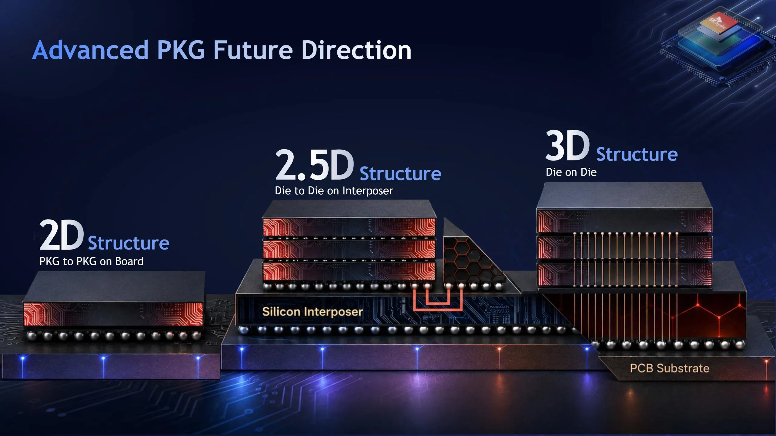
The third layer is 3D integration, stacking HBM and a compute die vertically. The presentation showed a future vision of placing HBM on top of a compute die. However, it did not disclose a product name, structural details, or the generation in which it would be introduced. Hybrid bonding, CoWoS or EMIB, and 3D integration are not technologies to be picked from a single menu; they operate at different levels.
Behind 2,048 I/Os, Signals and Power Compete for Area
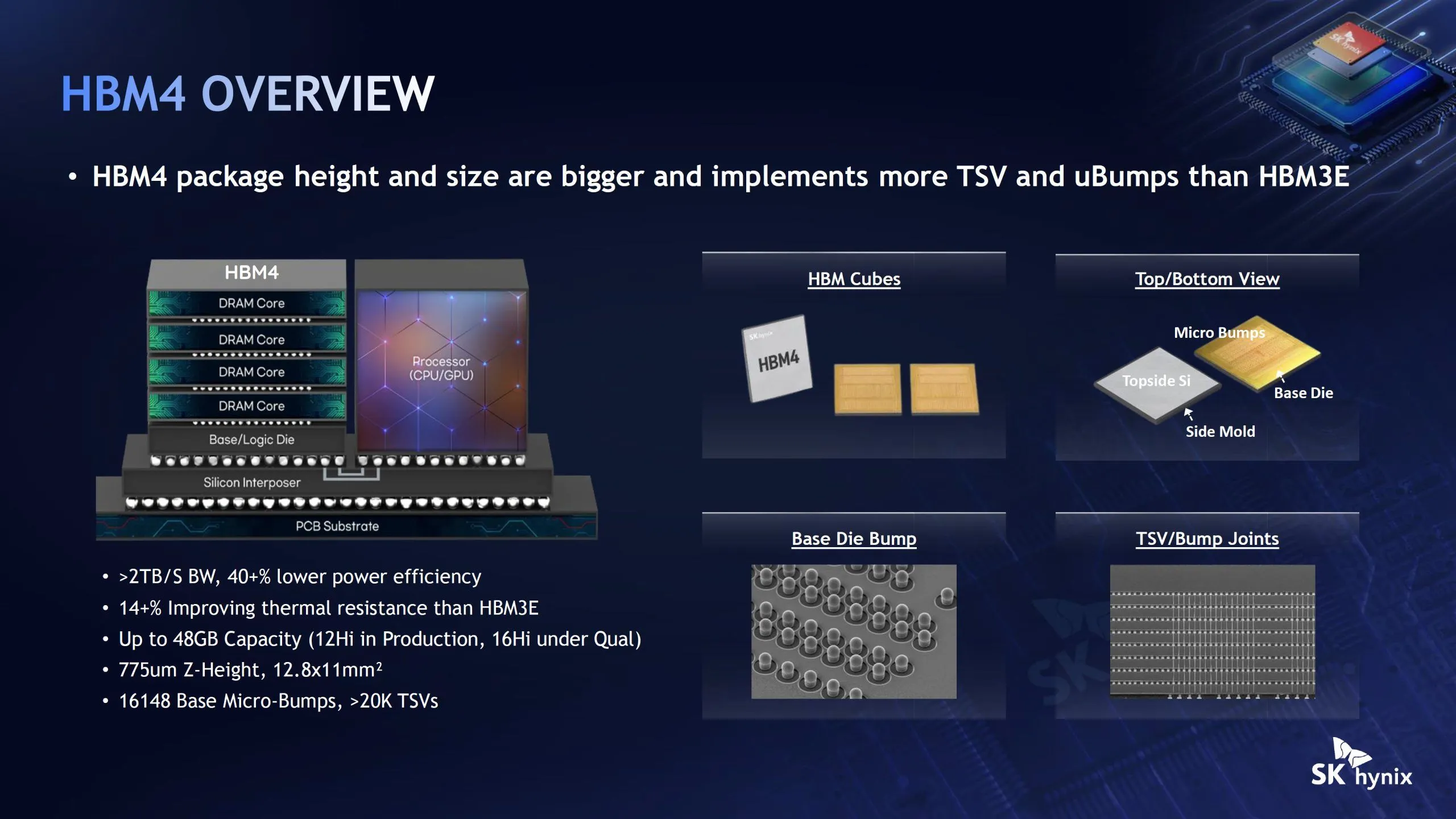
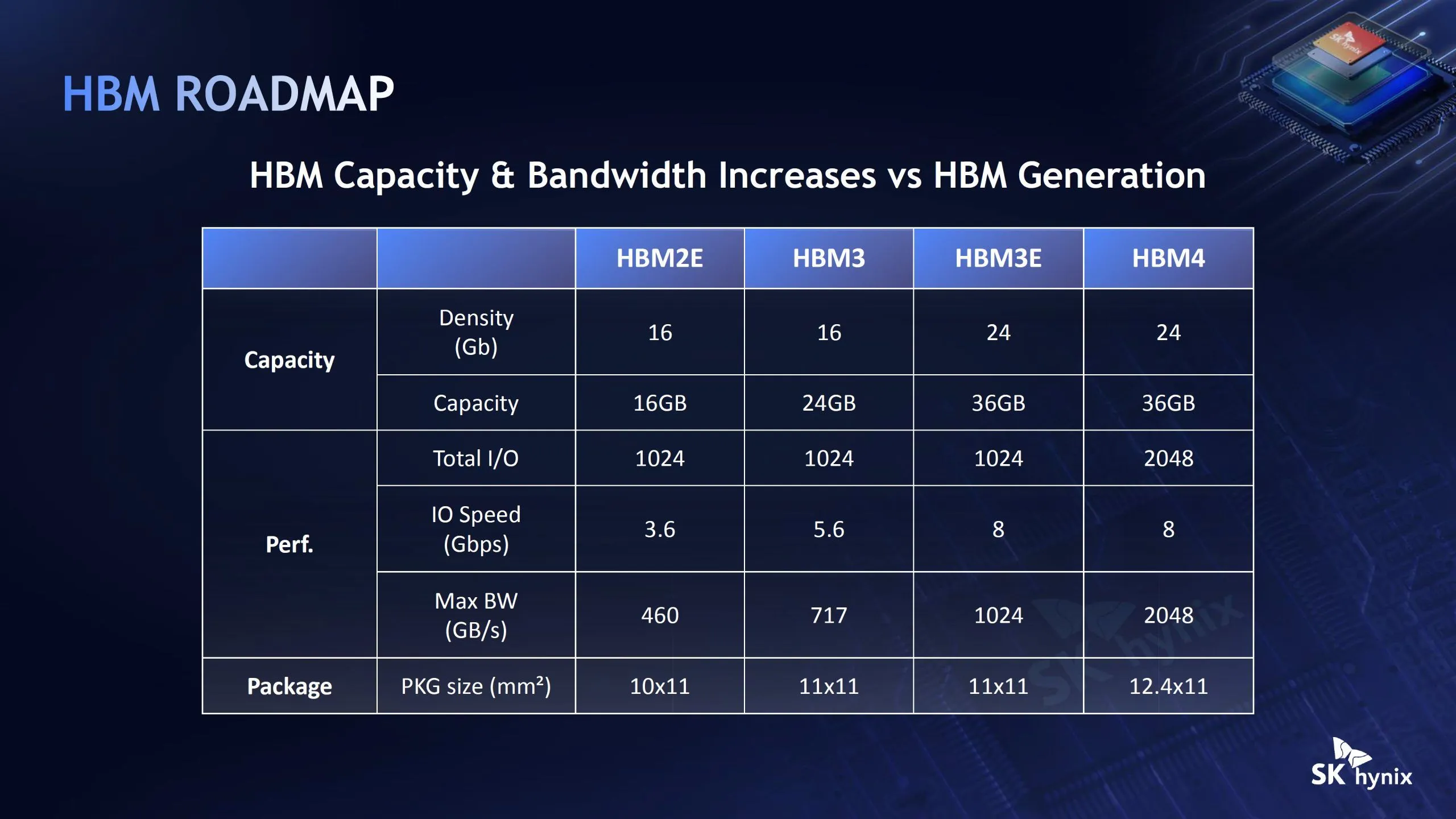
According to the slides, HBM4 delivers more than 2TB/s and up to 48GB, with 12Hi in mass production and 16Hi under qualification. The thickness is 775µm, with 16,148 microbumps on the base side and more than 20,000 TSVs. The HBM4 that SK hynix says is ready for mass production has 2,048 I/Os and runs at over 10Gbps. The company says power efficiency improved by more than 40% over the previous generation.
In the generational comparison on the slides, 2,048 I/Os is double the previous generation. More pins widen the data path, but on the underside of HBM, signal lines and power lines share the same area. Raising pin speed tightens signal-quality requirements, and the power delivery design that suppresses voltage fluctuation and wiring resistance constrains bandwidth. More than 20,000 TSVs and 16,148 microbumps indicate that the connections themselves have grown to a scale where they consume area and heat.
The presentation also explained that while bandwidth roughly doubles every two generations, the thermal load on existing processes and packages rises 2.2 times. Future measures cited include doubling the TSV count and raising I/O speed, and a concept was shown that incorporates an advanced logic process and distributes power TSVs across the power delivery network. None of these are product specifications, but they show that bandwidth and power delivery cannot be increased independently.
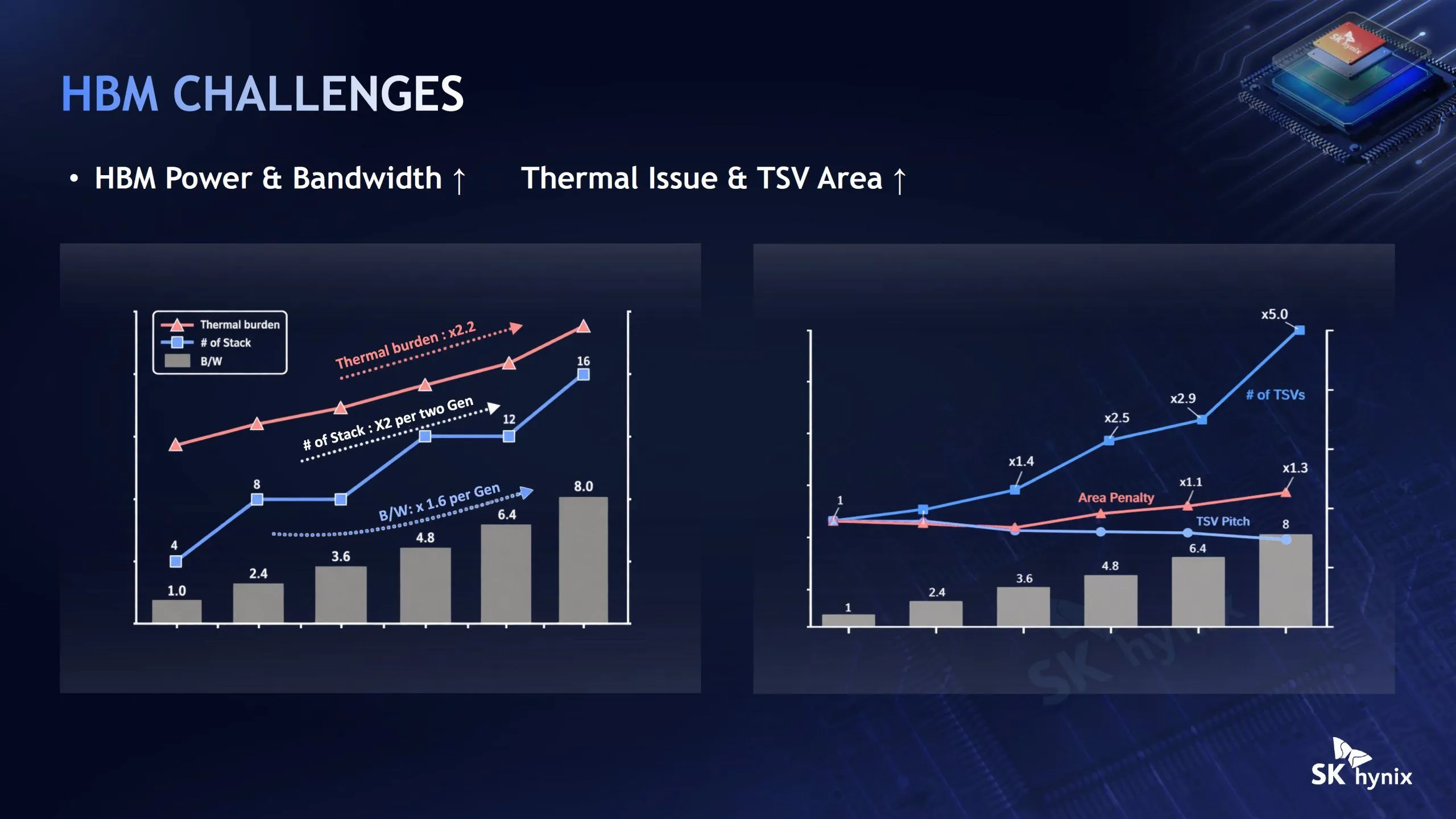
Beyond 16Hi, simply thinning dies to add layers makes it harder for heat to escape. Yet thicker dies leave less room within the 775µm height. The trade-offs among stack count, die thickness, and connection pitch must be solved within a single process.
MR-MUF for Mass Production, Hybrid Bonding Beyond 16 Layers
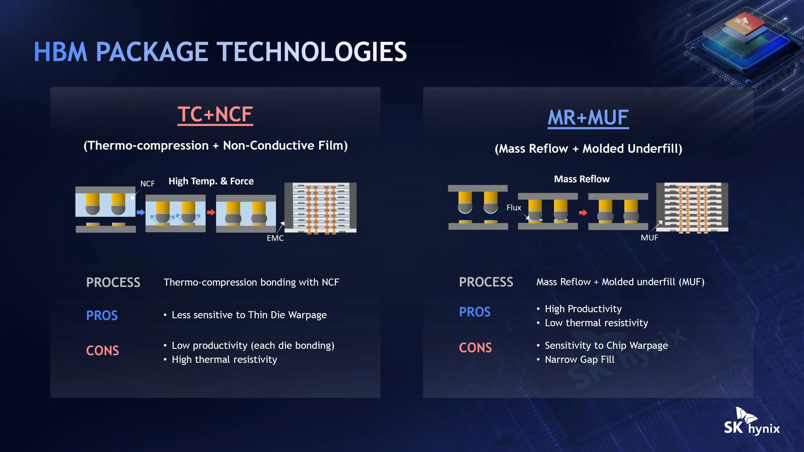
SK hynix's HBM4 mass production begins with the proven Advanced MR-MUF. This method bonds multiple dies together at once, then flows a liquid filler into the gaps and cures it. The company's official interview explains that it offers better process efficiency and heat dissipation than the conventional method of inserting film-type material between each layer. However, with 12-layer HBM3, warpage of the thinned dies became a problem for the original MR-MUF, and Advanced MR-MUF improved warpage control and heat-dissipation materials.
The slides characterized TC-NCF as resistant to die warpage but with higher thermal resistance and lower productivity, and MR-MUF as advantageous in productivity and thermal resistance but challenged by warpage and filling narrow gaps. This is not an absolute ranking of the methods. As stack count, die thickness, and connection spacing change, so does which of warpage, productivity, or thermal resistance becomes the limit.
Hybrid bonding joins copper and insulating layers directly, without microbumps. The Hot Chips material stated that, compared with MR-MUF, it allows core dies to be 24% thicker and TSV pitch to shrink below 18µm. It also reportedly cuts thermal resistance by 35% even with more layers stacked. However, the comparison structure and evaluation conditions cannot be confirmed from the public pages, so the 35% figure cannot be applied to every HBM.
Bonding copper directly to copper requires bonding surfaces to be flat and clean to a high standard. Small alignment errors or a single particle can cause connection failures, so the open question is whether the thermal performance shown in the presentation can be carried over to mass-production yield.
Thermal measures are advancing in parallel with the change in bonding surfaces. SK hynix's iHBM places ICE, which conducts heat but not electricity, at the hot spot of the D2D PHY connecting the base die and compute die. The design lowers thermal resistance by 30% through a dedicated heat path, and the company plans to apply it to next-generation products including HBM5. A staged approach is visible: keep Advanced MR-MUF, release local heat, and then use hybrid bonding beyond that.
What EMIB's Appearance Means, and What It Doesn't Mean as a Contract
In 2024, SK hynix signed an MOU with TSMC to use TSMC's advanced logic process for the HBM4 base die and to jointly optimize the integration of HBM with CoWoS. EMIB's addition to the Hot Chips slides does not erase this official collaboration.
Intel offers EMIB as a 2.5D technology connecting logic to logic or logic to HBM. Instead of placing a large full-surface silicon interposer, it embeds silicon bridges at die boundaries where high-density wiring is needed. EMIB-T adds TSVs to those bridges to strengthen vertical power delivery paths.
A full interposer and local bridges differ in wiring flexibility and in how power is routed. Manufacturing processes and supply chains are not the same either. Customers therefore cannot switch from CoWoS to EMIB just before completion, and superiority cannot be decided by any single item such as maximum area or cost. On the HBM side, compatibility must be verified in advance against the compute die's wiring and power delivery conditions.
SK hynix and Intel did not announce an EMIB adoption contract, product name, or mass-production timing alongside the presentation. All that can be confirmed from the slide listing is that SK hynix includes multiple 2.5D methods among its targets for co-design. Concluding a shift from TSMC or adoption in Intel products would require customer qualification and a mass-production plan, which are missing.
With 3D, the Direction of Heat Removal Changes
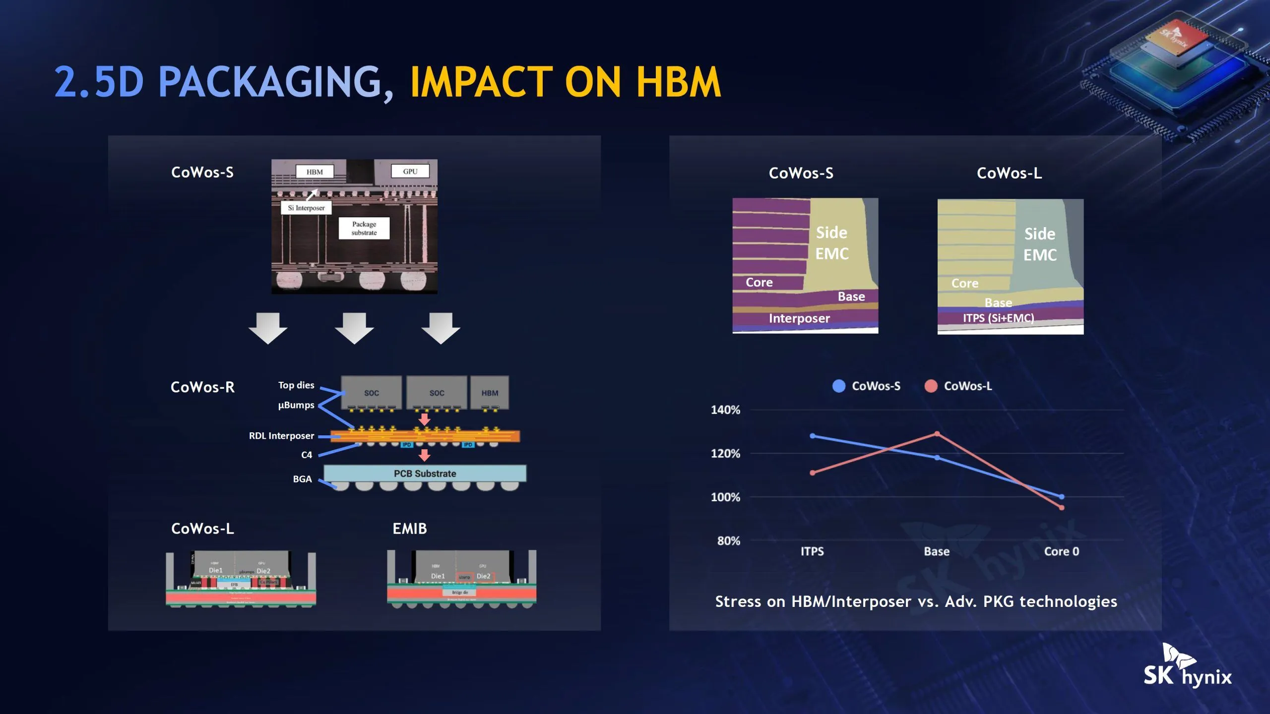
In 2.5D, HBM and the compute die sit side by side, making it easier to separate the paths that remove heat from the top surface of each. 3D integration can shorten connection distances, but it stacks the heat-generating logic and the temperature-sensitive DRAM on top of each other. If heat rising from the compute die passes through HBM, the cooling path must be reworked to match the stack structure.
That iHBM adds a dedicated heat path to the localized hot spot of the D2D PHY is because heat generation at the interface is already a problem in the side-by-side 2.5D structure. With 3D, local escape routes must be extended into cooling for the entire stack. The electrical advantage of shorter wiring and the disadvantage of closer heat sources arise at the same time.
Yield calculations change too. Known good dies can be screened before stacking multiple dies, but a defective die after bonding is hard to replace. With each added layer, the success of alignment, bonding, and inspection accumulates in the final product. Even if hybrid bonding works inside HBM, it does not necessarily mean the yield of the whole HBM-on-logic structure will immediately hold up.
The Hot Chips material showed the direction of 3D integration but did not give a product name or mass-production generation. The next things to watch are qualification by customers who adopt HBM-on-logic, and a structure that releases logic heat without passing it through the DRAM. When those two are published as product specifications, SK hynix's three-layer design will move from a research concept to a mass-production roadmap.