


Behind the scenes of a smartphone instantly completing facial recognition or voice processing, massive amounts of data are constantly shuttling back and forth between the processor and memory. Inside a chip, the computation itself surprisingly consumes very little energy. What devours the most power and is the primary source of heat generation is the process of moving data to the site of computation. As the number of parameters in AI models balloons from billions to trillions, the traditional von Neumann architecture—in which compute units and memory are physically separated—is running into fundamental walls of data transfer latency and power consumption.
As an approach to breaking through this bottleneck, "in-memory computing (IMC)," which completes calculations within the memory cell itself, has come to the fore. In particular, architectures using "memristors" (resistive RAM, or RRAM)—non-volatile memory devices that analogically change their resistance value when voltage is applied and retain that state even when powered off—are gaining attention as a foundation for executing massive matrix-vector multiply-accumulate operations in parallel and at extremely low power.
The Physical Dilemma at the Heart of Model Miniaturization: "Depthwise Convolution"
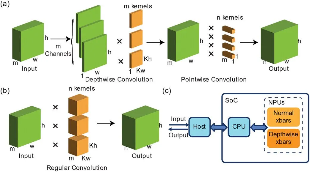
IMC is an excellent concept, but it is not a universal solution for every type of computation. For operations like fully connected layers or standard convolution, where data is densely shared and reused many times, the crossbar array (a grid-like circuit network) formed by memristors delivers overwhelming efficiency. However, mobile devices and other platforms with strict power and thermal constraints have no choice but to adopt lightweight AI networks (such as MobileNet) that dramatically reduce the amount of computation. The core operation underlying this lightweight architecture is "Depthwise Convolution (DWC)."
Whereas standard convolution integrates information from all input channels (for example, all of an image's RGB channels) to produce a single output, DWC applies a completely independent spatial filter to each input channel. To use a paint analogy: rather than mixing multiple colors together on a palette, this is a processing structure in which red is applied with a red brush and blue with a blue brush, painted separately onto the canvas without interfering with each other. This independence dramatically reduces the model's computational load.
However, this independence between channels causes a serious mismatch with the physical structure of analog IMC. When DWC operations are directly mapped onto a conventional grid-shaped crossbar array, each piece of input data accesses only a specific filter, leaving most memory cells as blank zones uninvolved in the computation. Memory utilization drops to just a few percent, parallel data processing is hindered, and as a result, the inherent benefits of IMC are lost—a physical dilemma that has long persisted.
Zigzag Wiring Delivers a Near-Optimal ~100% Memory Utilization
The research team that solved this physical inefficiency by transforming the wiring structure on silicon itself is a collaboration between US semiconductor startup TetraMem and South Korea's SK hynix. Together they developed a memristor-based system-on-chip (SoC) prototype that includes a hardware accelerator dedicated to DWC.
The root of the problem lay in the fact that the selection lines (SEL) used to read and write data were laid out straight, either horizontally or vertically, on the chip. With straight-line wiring, when the weight data of DWC's independent filters is mapped onto the array, only a small portion of cells located along the diagonal of the circuit can be activated with a single command.
The team devised a proprietary DWC-dedicated crossbar (dw-xbar) in which the selection lines controlling the transistor gates are wired in a "zigzag" pattern that folds back diagonally. When a specific selection line is turned on, a group of cells arranged along the physical diagonal of the circuit are simultaneously activated. This architecture makes it possible to multiply only the necessary weights in parallel for the signal flowing from a single input line (word line), without passing through any wasted cells. Even with DWC's irregular access pattern, this special structure consistently keeps memory utilization close to 100%.
A Command Center Uniting Heterogeneous Cores—A Heterogeneous Structure Controlled by RISC-V
This optimization of computational efficiency brought about a dramatic reduction in the chip's overall power consumption. The prototype SoC developed in this study adopts a heterogeneous design equipped with a total of 10 neural processing units (NPUs). Of these, one is the zigzag-wired crossbar dedicated to DWC, while the remaining nine are standard crossbars that handle operations such as the 1×1 pointwise convolution (PWC) that follows DWC.
What seamlessly coordinates this complex arrangement of heterogeneous cores is a RISC-V-based CPU embedded within the chip. Modern AI models are not composed of a single type of operation but consist of a series of diverse processing layers. The embedded CPU acts as a command center that directs the flow of data, dynamically assigning tasks to the optimal hardware unit for each layer of the network. When a DWC layer arrives, it routes data to the zigzag-wired NPU; for standard convolution layers, it assigns processing to the remaining nine NPUs. Furthermore, it executes fine-grained control that spans the hardware-software boundary in real time, including adjusting the quantization scale of input data and correcting for errors specific to analog computation.
In measured tests, the NPU cores on the chip recorded an extremely high power efficiency of 21.3 TOPS/W (21.3 trillion operations per second per watt) when driven at 100MHz.
Considering that NVIDIA's A100 GPU, currently the workhorse of AI development in data centers, achieves a power efficiency of only about 2.08 TOPS/W even under optimized conditions, this chip already achieves more than 10 times greater energy efficiency. This figure is on par with, or even exceeds, the 17.2 TOPS/W reported by SRAM-based IMC chips manufactured on a cutting-edge 28nm process. Given that the prototype was fabricated on a 65nm process—several generations older—this strongly underscores the fundamental superiority of the architecture.
| Item | Data Center GPU / Conventional Crossbar | This Study's Heterogeneous SoC (DW NPU) |
|---|---|---|
| Computing method | Processor-memory separated / straight-line wiring | Analog in-memory computing / zigzag wiring |
| Memory utilization during DWC processing | Low data reuse leaves many cells idle | Diagonal wiring eliminates waste, improving to ~100% |
| Power efficiency for INT8-equivalent processing | About 2.08 TOPS/W (e.g., NVIDIA A100) | 21.3 TOPS/W (at 100MHz operation) |
| Weight data retention during inference | Lost when power is off, requiring reload | Retained without power via non-volatile memristors |
The reduction in computational load achieved by introducing DWC is also mathematically clear. The ratio of the number of multiply-accumulate (MAC) operations between standard convolution and Depthwise-Separable Convolution (DSC), which uses DWC, is formulated as follows.
This equation means that as the number of output channels ($n$) or the area of the spatial filter () increases, the value of the equation approaches zero, indicating that DSC dramatically compresses computational cost. Applying representative conditions of a 3×3 filter size and 32 channels, the amount of computation is reduced to roughly one-seventh of the normal amount.
Dynamic Correction Technology That Tames Analog-Specific "Fluctuations"
While analog circuits boast extremely high efficiency, they carry the inherent fate of being vulnerable to environmental noise and manufacturing variation between devices. Unlike the "0" or "1" of digital circuits, the resistance value written to a memristor is a continuous physical quantity, so minute errors during programming accumulate and ultimately degrade the accuracy of the final inference.
In this study, the researchers addressed these fluctuations from both the manufacturing process and circuit design perspectives. On the manufacturing side, SK hynix's fab adopted an amorphous (hafnium oxide) thin film for the switching layer, employing precise control to keep the concentration of oxygen vacancies uniform even after high-temperature processing.
Furthermore, on the circuit design side, they incorporated a dynamic correction mechanism using multiple subarrays. When a numerical value is written to the first memory cell, the system reads the physical error that occurs, calculates a scaling coefficient that precisely cancels out that error, and writes it to an adjacent second cell. By summing the outputs of these two cells, they were able to stably secure an effective weight precision of about 4 bits in hardware.
The team built a software pipeline that mimics the behavior of the custom-designed hardware and ran a person-detection task (Visual Wake Words) based on MobileNetV1 on the chip. The result showed that the actual hardware inference accuracy reached 80.36%. This is on par with the accuracy of a 4-bit quantized model computed without error in software (79.34%), proving that the non-idealities specific to analog computation have been fully controlled at a practical level.
The Strategic Significance of "Memory That Doesn't Just Remember" as Envisioned by SK hynix, the HBM Champion
One aspect of this joint research that should not be overlooked is the industrial context of South Korea's SK hynix's deep involvement. The company currently leads the market for high-bandwidth memory (HBM), which is indispensable to NVIDIA's AI semiconductors, and is one of the companies benefiting most from the global AI boom. However, HBM is ultimately a brute-force approach of "placing an ultra-fast data warehouse right next to the processor," and it does not completely solve the fundamental problem of power consumption.
SK hynix is already looking ahead to the next-generation computing paradigm that lies beyond HBM. That is the pursuit of memory that not only "remembers" data but also "computes" on its own. This analog IMC approach, which resembles the neural networks (neuromorphic) of the brain, demonstrates its true value not on the cloud side, which consumes large amounts of power, but on the edge side, where power constraints are severe. This chip bears the clear strategic imprint of SK hynix's ambition to leverage its strength in conventional memory manufacturing while seizing leadership in a new computing paradigm.
The Next Milestone Toward Autonomous Edge AI
If the ultra-low-power AI inference enabled by this chip is put into practical use, the devices around us will undergo a dramatic evolution. For example, in small drones where battery weight and capacity directly impact flight time, systems could be realized that instantly detect and autonomously avoid obstacles onboard the aircraft, without transmitting video to the cloud. Or AR smart glasses, which allow only millimeters of battery space, could continuously recognize objects in the user's field of view in real time, all day long. Furthermore, a world where AI is truly ubiquitous could unfold—one that includes smart home cameras capable of detecting human presence with extremely high accuracy even in environments completely cut off from network connectivity.
This SoC development is not merely a proof-of-concept for circuit design. The greatest breakthrough of this project lies in the fact that the team integrated a special memristor structure into a commercial foundry's mass-production process and thoroughly verified end-to-end operation on an actual AI task.
This approach, which dissolves the boundary between computation and memory, forms the foundation for a future in which small, battery-powered edge devices can autonomously run advanced AI without relying on the computational power of massive data centers. Engineering challenges remain to be solved, such as developing a complete automatic compiler for analog IMC and scaling up to even more multi-layered networks. But the physical path toward freeing AI from the curse of the von Neumann bottleneck—which has long dominated computer science—is certainly coming into focus.