

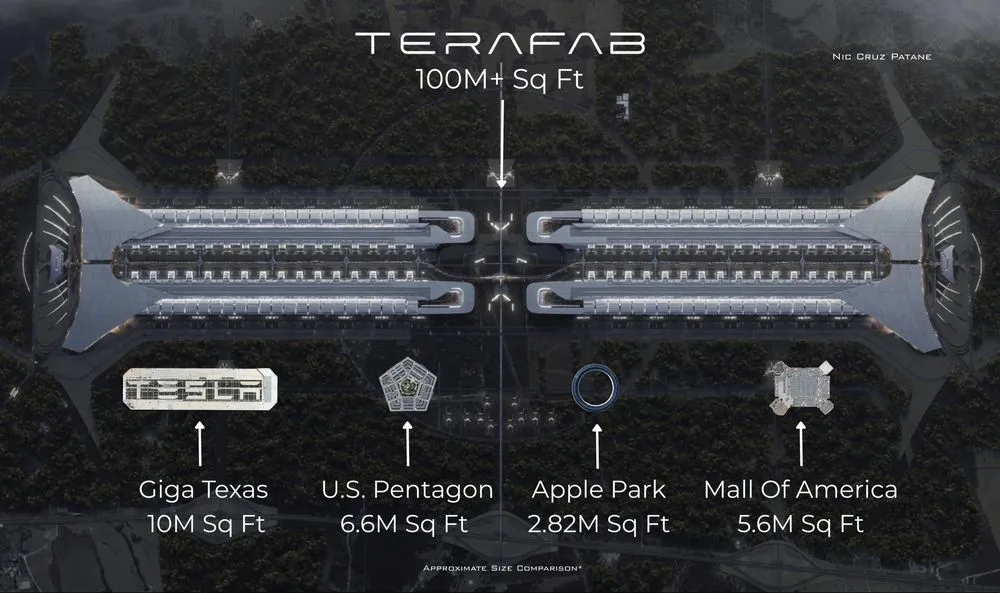
A diagram comparing the size of the semiconductor fab "Terafab," planned by SpaceX and Tesla, against Giga Texas, the Pentagon, Apple Park, and the Mall of America—all placed on the same plane—has been spreading on X. The plan SpaceX unveiled on August 6, 2026, calls for over 100 million square feet of "manufacturing space." Rounding and adding the published figures for the four facilities yields roughly 24.9 million square feet, meaning Terafab's number is about four times that combined total.
However, this diagram cannot tell us the finished building's exterior shape. What's being compared is mainly total floor area, not the footprint as seen directly from above. We need to separate the staggering scale conveyed by the diagram from the design, which has not yet been finalized.
Even the Four Facilities Combined Are Only a Quarter of Terafab
The diagram published by Nic Cruz Patane on August 6 arranged the outlines of the four facilities inside a large rectangle representing Terafab. Tom's Hardware also covered this comparison on August 9. Lining up the rounded figures from each facility's official materials gives the following relationships:
| Facility | Published Area | Meaning in Source Material |
|---|---|---|
| Terafab | Over 100 million sq ft | Manufacturing space (planned) |
| Giga Texas | Over 10 million sq ft | Factory floor area |
| Pentagon | 6.5 million sq ft | Total building floor area |
| Apple Park | 2.8 million sq ft | Main building floor area |
| Mall of America | 5.6 million sq ft | Total building floor area |
The rounded figures for the four comparison facilities add up to 24.9 million square feet. Dividing Terafab's 100 million square feet by this total gives roughly a factor of four. Converted to square meters, this comes to about 9.29 million square meters—but that's merely a floor-area conversion.
Moreover, the figures in the table aren't defined on strictly equal terms. Giga Texas is listed as "over 10 million square feet," and the Apple Park figure refers to the main building, not the entire campus. While the diagram is useful as a tool for grasping a sense of scale, it isn't a surveyed comparison of physical structures.
What the Floor Plan Doesn't Reveal About "Manufacturing Space"
SpaceX's announcement describes Terafab as having "manufacturing space exceeding 100 million square feet." However, it doesn't disclose the number of building stories, the dimensions of individual buildings, or the actual footprint on the site. A multi-story design could pack the same floor area onto a smaller plot of land, while a single-story design would result in a larger footprint. Therefore, translating 100 million square feet into a single rectangle involves architectural assumptions not found in the official materials.
Nor can we assume all of this "manufacturing space" is clean room. The scope SpaceX cites includes not only advanced logic and memory manufacturing but also packaging and testing. A June prospectus went further, outlining a vision of consolidating even photomask design into a single closed-loop factory. According to SpaceX's explanation, the manufacturing space exceeding 100 million square feet includes processes of very different character. It cannot all be read as clean room area.
Multiple Manufacturing Processes Contained Within the 100 Million Square Feet
Terafab is planned to produce chips for inference in Tesla's humanoid robot "Optimus" and its self-driving car "Cybercab," as well as high-power chips for SpaceX's orbital data centers. SpaceX explains that by manufacturing logic and memory and repeatedly cycling through assembly and testing at the same site, the time needed to feed design changes back into manufacturing can be shortened. The manufacturing space described in the official materials encompasses these multiple processes. However, the area allocation by process has not been disclosed.
The "1 TW/year" figure listed on the official site is also not the power the factory consumes. In SpaceX's prospectus, it represents a long-term target for the annual production capacity of computing hardware. Neither the conversion formula linking floor area to 1 TW, nor the number of wafer starts, has been disclosed. Securing a large building does not by itself translate into large production capacity.
Numbers That Should Be Confirmed Before the 100 Million Square Feet Figure
SpaceX itself lists the possibility that Terafab may not succeed as a risk factor in its prospectus. As of June 2026, individual development schedules and milestones were undetermined, and neither Tesla nor Intel had an obligation to remain committed to the project. Even after completion, a significant portion of computing hardware is expected to be sourced externally.
What was confirmed in the August announcement was the construction site in Grimes County, Texas, and a plan for SpaceX and Tesla to invest roughly $16.8 billion in the initial phase. A policy of employing at least 3,000 people was also indicated. However, the final building layout, clean room floor area, and process generation remain blank.
The comparison diagram conveyed the magnitude of Terafab at a glance. To gauge whether the plan will translate into actual semiconductor supply capacity, we'll need to wait for the architectural drawings, wafer-start capacity, mass-production node, yield, and first-wafer date that come next. Only once these are all in place can we properly assess the relationship between the planned scale of 100 million square feet and actual manufacturing capacity.