

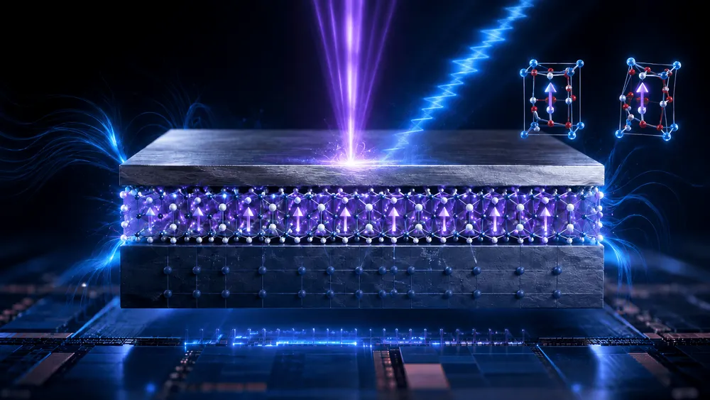
Titanium dioxide (), familiar as a main ingredient in sunscreen and white pigments, transforms into a material capable of retaining an electrical 'memory' when its thickness is cut down to 3 nanometers or less. This phenomenon, reported in the journal Science in August 2026, overturns more than half a century of conventional wisdom regarding the thinning of ferroelectric films. The established rule had always been: thin the film, and ferroelectricity disappears. Yet in , the thinner the film gets, the stronger the polarization becomes.
Why Ferroelectricity Vanishes as Films Get Thinner
A ferroelectric is a material that possesses spontaneous electric polarization even without an applied external field, and whose polarization direction can be reversed by an electric field. Ever since Joseph Valasek, a graduate student at the University of Minnesota, first discovered this phenomenon in Rochelle salt in 1920, ferroelectrics have been studied as foundational materials for nonvolatile memory and sensors.
However, ferroelectric thin films face a fundamental barrier. As a film becomes thinner, the polarization charge appearing at the surface is not perfectly screened, generating an internal electric field (the depolarization field) that points opposite to the polarization. This depolarization field destabilizes the polarization, and below a certain critical thickness, the ferroelectric phase itself disappears. In perovskite oxides (such as barium titanate—the 'classic' ferroelectrics), this critical thickness has been understood to be on the order of a few unit cells. In 2004, Fong and colleagues confirmed ferroelectricity in lead titanate films down to 3 unit cells (about 1.2 nm), a result that approached the apparent limit for perovskite systems.
The problem is that modern semiconductor devices operate precisely at that scale. In an era when transistor gate lengths are measured in single-digit nanometers, a ferroelectric that only works when thick is of little practical use.
A Reversed Approach: 'Thin It Down to Make a Ferroelectric'
Professor Sayeef Salahuddin's group at UC Berkeley approached this problem from the opposite direction. Rather than asking how thin an existing ferroelectric can be made, they asked whether a material that is not a ferroelectric to begin with might become one when thinned.
This idea traces back to a prior study the same group published in Nature in 2020. They grew zirconium-doped hafnium oxide () thin films directly on silicon and demonstrated ferroelectric switching at a thickness of 1 nm. That work yielded an important clue: in -based thin films, unlike in perovskites, an 'inverse size effect' was at work, in which polarization distortion actually increases as the film gets thinner.
This inverse size effect has a structural origin. In the fluorite-type structure that and adopt as thin films, the ferroelectric orthorhombic phase (space group ) has higher symmetry than the monoclinic phase (space group ) that is stable in bulk form. In perovskites, surface energy acts to stabilize the higher-symmetry paraelectric phase, whereas in fluorite-type structures, surface energy acts to stabilize the non-centrosymmetric phase. Thinning the film does not destroy polarization—it actually creates it.
In the 2020 result, however, doping with 20% zirconium was still necessary. The present study pushed the question one step further: does there exist a material in which the ferroelectric phase emerges simply by thinning a pure dielectric, with no doping required at all?
Crystal Distortion Begins at 3 Nanometers
The research team chose . The reasoning was clear: is a dielectric already widely used in semiconductor manufacturing processes, and atomic layer deposition (ALD) techniques for growing it are well established. There is real potential to repurpose a material already entrenched in industry as a pigment, catalyst, and UV absorber directly for ferroelectric devices.
Koushik Das, a UC Berkeley graduate student and the lead author of the study, and colleagues used ALD to grow thin films with thicknesses of 1–10 nm at temperatures below 400°C, on substrates of silicon, silicon dioxide (), and amorphous carbon. The fact that growth temperatures stay below 400°C means high compatibility with existing CMOS manufacturing processes.
A decisive change appeared right around a thickness of 3 nm. Linear-polarized X-ray absorption spectroscopy performed at the Advanced Light Source (ALS) at Berkeley Lab showed that in samples thicker than 3 nm, the absorption spectrum did not depend on direction—indicating an isotropic, centrosymmetric crystal structure. Below 3 nm, however, the absorption clearly varied with direction, revealing the emergence of anisotropy associated with polarization distortion. Christoph Klewe, a researcher at ALS, noted, " behaves differently from other ferroelectrics. Normally, thinning a film weakens the distortion, but in this material, the distortion increases as the thickness decreases."
Second harmonic generation (SHG) measurements at the Molecular Foundry independently confirmed this symmetry breaking. SHG is an optical phenomenon that produces a signal only when a material lacks inversion symmetry. The SHG signal increased sharply in samples 3 nm and thinner, clearly pinpointing the threshold for the structural transition.
Archana Raja, a staff scientist at Lawrence Berkeley National Laboratory, explained, "Since atoms are literally being displaced as part of the structural transition, we are directly measuring the crystal distortion."
Electrical Measurements Confirm 'Genuine' Ferroelectricity
Symmetry breaking in the structure alone is not sufficient proof of ferroelectricity. Unless the polarization can be reversed by an electric field, the material cannot properly be called a ferroelectric. The research team combined three types of electrical measurements to verify this point.
Using piezoresponse force microscopy (PFM), the team applied voltage to the film surface through a scanning probe tip and observed local reversal of polarization. Polarization–electric field (P–E) hysteresis measurements yielded the classic butterfly-shaped loop characteristic of ferroelectrics. Additionally, PUND (Positive-Up-Negative-Down) measurements confirmed that the observed current genuinely originated from polarization reversal, ruling out artifacts from leakage current or capacitive effects.
Taken together, these measurements show that ultrathin transitions from its normal centrosymmetric fluorite-type structure into a distorted orthorhombic structure, exhibiting a ferroelectric phase with polarization that can be switched by voltage. The polarization points in a direction tilted relative to the film plane, and the editors at Science noted that this 'slanted polarization' enables in-plane polarization switching, which is advantageous for applications in integrated electronics.
| Item | Perovskite systems (, etc.) | Fluorite-type (2020) | Fluorite-type (this study) |
|---|---|---|---|
| Ferroelectricity in bulk | Present | Absent (emerges with doping) | Absent (emerges only through thinning) |
| Response to thinning | Polarization weakens and vanishes | Polarization increases (inverse size effect) | Polarization emerges and increases |
| Concept of critical thickness | Present (a few unit cells) | Essentially absent | Instead, an 'emergence threshold' (about 3 nm) |
| Thinnest confirmed ferroelectricity | ~1.2 nm (3 unit cells) | 1 nm | 1 nm (~2 unit cells) |
| Growth temperature | High (typically 600°C or above) | 250°C (ALD) | Below 400°C (ALD) |
| Direct growth on Si substrate | Difficult | Possible | Possible |
| Doping requirement | Not required (intrinsic ferroelectric) | Zr doping required | Not required |
Close Proximity to Manufacturing Reality
The engineering significance of this discovery does not lie merely in the novelty of the material. is a 'known material' to semiconductor fabs. The ALD equipment, precursor gases, and process conditions all already exist on production lines. There is no need to qualify an entirely new material from scratch.
Moreover, the thin films in this study exhibited ferroelectricity not only on crystalline silicon but also on amorphous and amorphous carbon. This independence from substrate crystallinity is an important advantage for applications in three-dimensional integration and back-end-of-line (BEOL) processes.
Professor Salahuddin remarked, "The fact that a dielectric material can undergo a ferroelectric phase transition when thinned to the atomic scale opens up intriguing possibilities—both for the physics of phase transitions and for the study of polarization distortion in an entirely new class of materials."
Remaining Questions
This study demonstrates the existence of the ferroelectric phase and the conditions under which it forms, but its performance as a practical device has not yet been verified. Properties required for memory devices—such as switching endurance, polarization reversal speed, and suppression of leakage current—remain subjects for future work.
Furthermore, a complete theoretical explanation for the physical origin of the 3 nm threshold has not yet been established. While the framework in which competition between surface energy and elastic strain gives rise to the inverse size effect has been proposed for -based systems, further theoretical work will likely be needed to clarify mechanisms specific to (for instance, its relationship to the fact that fluorite-type is inherently a metastable phase at ambient pressure).
The research team's next goal is to build a 'library' of materials in which new functionality emerges through thinning. As Das put it, "When we want to build a device, we'd like to be able to choose different materials depending on the device architecture." The search for ferroelectrics is shifting from the question of "how thin can we make known ferroelectrics" to "what will we discover by thinning unknown materials."