

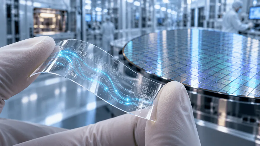
Imagine a chip with microscopic light pathways that bends like a transparent film. On September 3, 2026, the Massachusetts Institute of Technology (MIT) announced, together with NY CREATES, a semiconductor research and development organization in New York State, a fabrication technique for photonic integrated circuits that are both flexible and transparent. Its defining feature is that the circuits are made not as small individual chips but at the scale of 300 mm diameter wafers, the size used in semiconductor manufacturing. The results were published in Optica, Volume 13, Issue 9.
Silicon photonics uses semiconductor manufacturing technology to integrate circuits that guide and control light onto a chip. Conventional chips are supported by a thick silicon substrate, which makes them rigid and poorly transmissive to visible light. That has limited their use in applications such as conforming to curved surfaces or being placed where they do not block a person's view. This research aims to remove that limitation by taking advantage of the ease of handling silicon substrates during fabrication, then removing the supporting substrate at the end.
The research is led by Jelena Notaros, an associate professor in MIT's Department of Electrical Engineering and Computer Science (EECS) and a member of the Research Laboratory of Electronics (RLE). The first author is EECS graduate student Tal Sneh, and the co-authors are Andres Garcia Coleto, Milica Notaros, and NY CREATES' Thomas Dyer and Kevin Fealey.
Removing the silicon substrate to leave a thin photonic layer
Fabrication starts with an ordinary rigid silicon wafer. Using semiconductor manufacturing equipment at NY CREATES' Albany NanoTech Complex, the team forms waveguides, which serve as light pathways, and an oxide layer surrounding them. Next, a temporary supporting silicon wafer is bonded to the top surface and the whole assembly is flipped over. While the thin circuit layer is supported in this way, the original silicon substrate is removed from the back side.
Substrate removal combines industrial thinning with selective chemical etching. The silicon is first thinned, and the remaining portion is then removed by a method that is gentle on the photonic layer. A transparent polyester film is attached to the remaining thin film of waveguides and oxide, and when the temporary support wafer is detached, a transparent, bendable structure is obtained.
A distinction about thickness is needed here. The thickness of a few micrometers refers mainly to the functional layer consisting of waveguides and oxide, not to the total thickness of the finished chip including the support film. The paper's fabrication process describes a 50 µm polyester film, and the finished structure also includes this film and an adhesive layer.
Nor is this a technology that turns silicon itself into a transparent material. It removes the thick silicon support substrate used to build the photonic circuits and transfers the necessary thin-film layers to a transparent support.
Managing stress to keep a large-diameter thin film intact
The difficulty lies in keeping the thin film flat even after the support substrate is removed from a wafer as large as 300 mm. If stress during fabrication causes the wafer to warp, removing the substrate becomes harder. The thin film may also ripple or crack on the manufacturing line.
To limit stress, the research team adopted low-temperature processes at or below 500°C and adjusted both the method of removing silicon and the order of the steps. Beyond using high-precision processing equipment, deciding at which stage and by what means the thinned structure is supported became a key factor in making the fabrication work.
The result shows that existing semiconductor manufacturing technology can be used to process transparent, flexible photonic circuits at wafer scale. However, demonstrating wafer-scale fabrication is a separate stage from achieving stable yields and manufacturing costs for a commercial product. The fact that the process works at 300 mm alone does not mean mass production is ready.
Thousands of bends withstood, but performance while bent is a separate question
The team evaluated the fabricated chips for waveguide optical properties, durability under repeated bending, and transparency. For optical properties, they used waveguides of different lengths to examine factors such as light propagation loss.
In the bending tests, a single chip was repeatedly wrapped around cylinders of different diameters. According to MIT's announcement, no performance degradation was observed after thousands of bends in tests that included a cylinder about as thick as a small screw. On the other hand, performance degradation was seen after wrapping the chip a few times around a thinner toothpick.
| Bending test condition | Repetitions | Reported effect on optical performance |
|---|---|---|
| Cylinders of different diameters, including one about as thick as a small screw | Thousands | No degradation observed |
| Wrapping around a toothpick | A few | Degradation observed |
The number of repetitions and the descriptions of thickness are based on MIT's announcement. (MIT News)
However, maintaining performance after repeated bending is not the same as maintaining optical performance while bent. The paper explicitly states that this study did not evaluate waveguide performance with the chip in a bent state. What the tests mainly confirm, therefore, is durability against bending; they do not demonstrate performance when the chip is fixed onto various curved surfaces.
The performance drop with the toothpick is also a result obtained for specific samples and a specific test procedure. It cannot be regarded as a material-specific failure limit, nor interpreted as a minimum bend radius common to chips of all dimensions.
Transparency tested with an optical setup that mimics the eye's imaging
To evaluate transparency, the team used an optical test setup called a "bionic eye," which mimics the eye's imaging. Assuming the chip is placed in front of the eye, they examined how much the image seen through it changes, and reportedly found that haze, or cloudiness, was small and noticeable image distortion was unlikely to occur.
This evaluation provides important baseline data for considering uses in which a transparent photonic circuit is placed in front of the field of view. On the other hand, obtaining a good image in an optical test setup does not by itself confirm how easy the view is during long-term wear or the safety of a finished display device.
The research team itself lists further improving transparency as a future challenge. "Transparent" should be understood not as meaning there is no light loss or effect on the image at all, but as meaning that the chip showed good transmission characteristics under the conditions evaluated.
Transparency and flexibility were already reported at a 2025 conference
The result fits within the Notaros group's ongoing research on wafer-scale flexible photonic integrated circuits.
An earlier paper published in Scientific Reports in 2024 reported mechanically flexible photonic integrated circuits made in a process using 300 mm wafers. That approach left the original silicon substrate thinned to about 30 µm, which differs from the present transparent structure in which the silicon support substrate is completely removed.
Later, at the 2025 academic conference Frontiers in Optics + Laser Science, the MIT and NY CREATES team had already presented a 300 mm wafer-scale fabrication technique combining transparency and flexibility. The abstract of the conference paper also notes that it demonstrated mechanical robustness, high transparency, and low optical distortion.
| Publication | Fabrication scale | Main content |
|---|---|---|
| 2024 Scientific Reports | 300 mm wafer | Flexible photonic integrated circuits made while retaining a thin silicon support layer |
| 2025 Frontiers in Optics + Laser Science | 300 mm wafer | Reported a fabrication technique combining transparency and flexibility, with evaluation results |
| 2026 Optica | 300 mm wafer | Reports a transparent, flexible fabrication platform and its characterization in a journal paper |
Based on the 2024 earlier paper, the 2025 conference abstract, and 2026 paper information. (Nature)
Therefore, it would not be accurate to describe the 2026 paper as the first time a chip that had only been flexible became transparent. Transparency and flexibility were also reported in the 2025 conference presentation, and the new paper follows from that line of development.
Applications in AR and wearables remain development goals
Applications cited by MIT include pilot visors for aircraft, augmented reality (AR) displays that follow a car's windshield, and unobtrusive health monitors that can be worn to fit the shape of the body. The idea is to embed thin circuits with optical functions in places where rigid flat substrates were hard to place.
However, the central results presented here are the fabrication technique and the evaluation of waveguides, bending durability, and transparency. They must be distinguished from demonstrations of image display by a finished AR visor or measurement performance by a health monitor worn on the body. MIT's announcement also describes adding more complex components and functions as a future goal.
When considering practical use, beyond the transparent photonic circuit itself, questions arise about how to configure light sources, light control mechanisms, detectors, and connections to electronic circuits for each application. These do not necessarily all need to be built on the same thin film, but designs are needed that preserve the benefits of transparency and flexibility when combined as a system.
Judging practicality will require validating functional integration and manufacturing and usage conditions
The next challenges the research team explicitly names are adding more complex functions, improving the light propagation efficiency of the waveguides, and improving transparency. Notaros has expressed an intention to eventually make the fabrication platform available to other research groups through collaboration with NY CREATES. However, this is a future outlook and does not mean it is already offered as a general fabrication service.
From a practical standpoint, beyond these baseline evaluations, the verification items for each application need to be organized. Examples include optical properties in a bent state, performance under changes in temperature and humidity, durability of the support film and adhesive layer, and transparency with light sources and electronic circuits attached. These do not mean defects have been found in the technology; they are conditions to be confirmed when moving from a component demonstration to a product.
On the manufacturing side, variation in characteristics by position on the wafer, the proportion of good devices obtained, reproducibility across multiple production runs, and costs including post-processing will determine practicality. Being able to process at wafer scale is an important step forward, but it alone does not guarantee that commercial mass production is viable.
The value shown by this research is that transparent, bendable photonic circuits can be made by leveraging the existing 300 mm semiconductor manufacturing infrastructure. It widens the manufacturing options for mounting on curved surfaces and placement that does not obstruct the field of view. The focus going forward will be whether optical performance and ease of handling can be maintained once the necessary functions are added.