

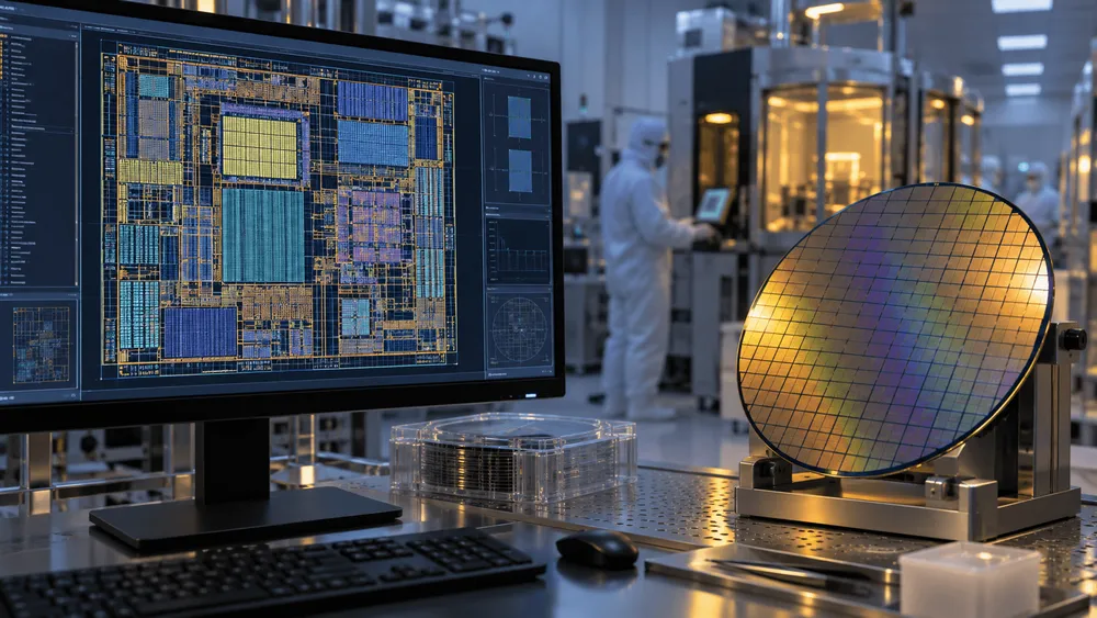
TSMC Co-COO Y. J. Mii has spoken about the limits AI faces in developing advanced semiconductor manufacturing processes. According to on-site reporting by Economic Daily News, Mii said at a discussion held at National Taiwan University on September 15 that he values AI in circuit design, but that development of nodes such as A14 still involves problems that existing materials and equipment cannot solve. Yet joint development of AI-assisted design tools for A14 is already under way. To make sense of this, it helps to separate two kinds of work: optimizing a chip's circuits, and establishing a manufacturing process that can actually build those circuits.
AI is good at searching for designs that can be evaluated
Mii spoke at a discussion co-hosted by National Taiwan University's Career Development Center, the TSMC Education and Culture Foundation, and United Daily News. Economic Daily News reported that he acknowledged AI's usefulness in programming and EDA (electronic design automation), saying circuit design has relatively clear inputs and outputs and involves large volumes of data, which makes it well suited to AI-assisted optimization.
Synopsys, which supplies design tools, offers a concrete picture of how this works. Its DSO.ai uses reinforcement learning to explore options in the design flow, aiming to improve PPA: power, performance, and area. It tries design candidates, evaluates the results, and searches toward better combinations. Both the subject matter and the way results are judged differ from asking a general-purpose chatbot a question in text.
In design, being fast is not always enough. Power consumption and area are also constraints, and the trade-offs among them determine which option is adopted. DSO.ai's simultaneous optimization of multiple goals supports that choice. Even when there are too many candidates for people to try one by one, AI can widen the search as long as the results can be compared.
The target is not limited to mature manufacturing processes, either. In an announcement on April 22, 2026, Synopsys said it is co-developing with TSMC AI-agent-assisted execution for Fusion Compiler using A14 NanoFlex Pro. The effort aims to find places at each stage of the design flow where signal timing can be improved.
The same announcement also touched on physical verification, which checks whether a design complies with manufacturing rules. Synopsys is developing AI assistance in IC Validator to speed up finding and resolving design rule violations. The inspection that looks for such violations is called DRC, and its role is to confirm that a design meets the manufacturer's requirements. These are presented as development efforts; they do not indicate a track record of volume production of A14 products, nor automation of the entire process development.
Supporting circuit design for A14 with AI is a long way from completing A14 manufacturing technology with AI alone. Even under the same node name, the problems being solved are different.
AI is already used on the manufacturing floor
TSMC is also bringing AI into its manufacturing processes. The "Quality and Yield Advancement" section of its 2025 annual report explains that it uses machine learning and other methods for yield analysis and process control. In addition to equipment fault detection, it lists virtual metrology and wafer defect inspection as uses. The report also describes efforts that combine generative AI with semiconductor manufacturing expertise to speed up the detection of process variation and related analysis.
In other words, AI use is already advancing in manufacturing-related work. But detecting anomalies in an existing process is not the same achievement as building an unknown process from scratch.
AI-driven exploration of design candidates, anomaly detection during manufacturing, and establishing a new manufacturing process each have different ways of confirming success.
| Task | Concrete example in public materials | What confirms the result |
|---|---|---|
| Exploring design candidates | DSO.ai optimizes PPA with reinforcement learning | How the power, performance, and area of design candidates change |
| Monitoring and analysis during manufacturing | TSMC uses AI for yield analysis, fault detection, and defect inspection | Whether anomalies are caught in real processes and wafers and help quality control |
| Establishing a new manufacturing process | Building the baseline process for A14 and improving yield and device/interconnect characteristics | Whether the devices and interconnects built meet target characteristics and the process holds together |
The table sorts the DSO.ai product description from Synopsys and sections 5.2.2 and 5.3.2 of TSMC's annual report by the object of each task. It is not an official TSMC classification or a ranking of AI performance, and the last column is our own summary of what each task is verified against. Because the methods and targets differ, the size of the effects cannot be compared side by side.
This distinction makes announcements that "AI accelerated chip development" easier to read. Whether the advance was in finding design candidates faster, catching manufacturing anomalies faster, or demonstrating a new process changes where the progress actually occurred. A shorter design effort does not automatically mean a shorter fab ramp-up.
A14 requires building and verifying the real thing
The A14 development challenges TSMC lists in its annual report include building a baseline manufacturing process and improving yield. Characteristics related to the resistance and capacitance of transistors and interconnects are also targets. It is not enough to choose a combination of circuits; the work includes confirming that what was built has the intended properties.
TSMC's lithography research also continues to work on reducing misalignment when circuit patterns are layered, as well as material defects. This describes lithography research as a whole, so it cannot all be treated as an A14-only challenge. Still, it shows that advanced process development spans everything from obtaining solutions on paper to achieving physical machining precision.
Even if AI proposes promising candidates, questions remain over whether they can be fabricated with the equipment and whether the devices built meet the required characteristics. Room to improve predictions with experimental data is one thing; whether experiments can be skipped is another. The constraints on materials and equipment that Mii described connect to this distinction.
The improvements A14 aims for are themselves substantial. In its 2025 announcement, TSMC set targets of up to 15% higher speed than N2 at the same power, or up to 30% lower power at the same speed. It aims for logic density gains of more than 20%, with production planned to begin in 2028. These are company plans, not a promise that the maximum speed gain and the maximum power reduction, which are measured under different conditions, can be achieved at the same time.
NanoFlex Pro is also presented as a mechanism that draws on experience in co-optimizing design and manufacturing technology. The design options customers use and the manufacturing technology behind them are linked. That is why there is no contradiction in using AI on the design side while continuing to refine real-world characteristics on the manufacturing side.
How to tell what work AI actually did
Economic Daily News reports that Mii compared AI to a "three-year-old Superman." The view is that even with powerful abilities, AI does not necessarily understand the consequences of its results, and that care is needed in handling research information that includes confidential material. Beyond technical performance, this raises the issue of what information to give AI and who decides whether to adopt its output.
The remarks do not support the conclusion that AI will never help in materials and process research. TSMC itself uses AI in manufacturing management, and design tool companies are developing support for A14. What the published efforts show is a present in which expectations for AI and the responsibility to demonstrate the process exist side by side.
In judging future results, it will help to look beyond the statement that AI was used and ask which tasks became shorter and under what manufacturing conditions the results were verified. If design improvements are linked to actual yield gains and those conditions are disclosed, it will become possible to evaluate concretely how far advanced semiconductor development times can be shortened.