

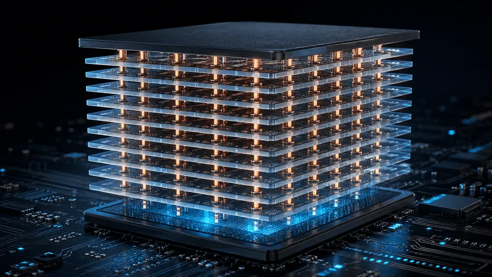
There isn't a day that goes by without the three letters "HBM" appearing in AI-related news. Even so, few people can explain in a single sentence what makes it different from ordinary memory, why it's essential for AI, or why it's so expensive. In fact, when NVIDIA unveiled its latest GPU, "Rubin," the first things discussed were memory capacity and bandwidth. The massive investments by the three major memory makers, and the DRAM price surge that has continued into 2026, all revolve around this stacked memory. This article builds up an explanation of HBM (High Bandwidth Memory)'s structure and manufacturing process from the ground up, so readers can understand—as a single continuous narrative—the competition now unfolding in the HBM4 generation, and its impact on Japanese companies and even the PCs we use ourselves.
How HBM Works: Stacking DRAM Like a High-Rise Building, Achieving Bandwidth Through 2,048 Wires
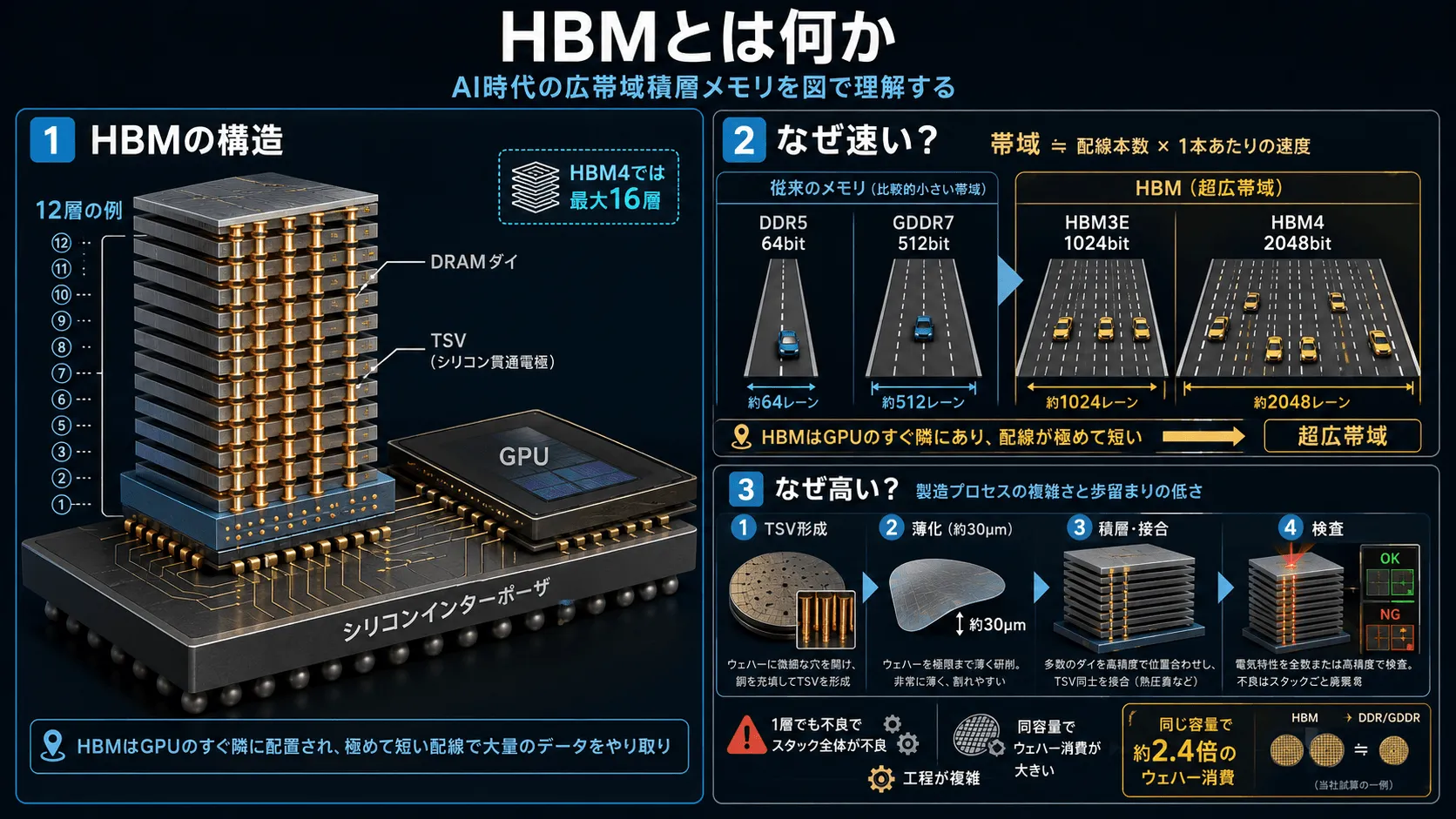
HBM is a stacked memory technology in which DRAM chips (dies) are vertically piled on top of each other and bundled together using microscopic electrodes that pass through the silicon. At the bottom sits a base die (logic die) responsible for signal control, and on top of it, core DRAM dies that store data are stacked—4, 8, 12, and in the latest generation, up to 16 layers. The layers are connected by copper pillars called TSVs (Through-Silicon Vias), with thousands of these vertical wires—each thinner than a human hair—running through a single stack. From the outside, the finished stack looks like a single component, but internally it resembles a high-rise building made of thin DRAM floors stacked vertically, with the TSVs acting as elevators running through every floor.
The reason this structure works so well comes down to the fact that memory bandwidth is roughly determined by "number of wires × transfer speed per wire." A PC's DDR5 memory exchanges data over 64 bits—that is, 64 wires—per module, and even GDDR7 for GPUs is limited by how many wires can be routed on a circuit board, capping out at 512 bits even in the top-tier GeForce RTX 5090. HBM, by contrast, offers an order-of-magnitude wider interface: 1,024 bits per stack through the HBM3E generation, and 2,048 bits with HBM4. Rather than adding more wires on the board's surface, HBM runs them vertically through the chip itself, securing a wire count that simply couldn't be achieved on a flat plane.
To use a road analogy: GDDR is like a highway with a few lanes on each side where cars race at 300 km/h, while HBM is an ultra-wide road that trades vehicle speed for 2,048 lanes. In fact, the speed per wire is actually lower for HBM—HBM4 runs at 8–10 Gbps, whereas the GDDR7 in the RTX 5090 runs at 28 Gbps (total bandwidth of 1,792 GB/s × 8 ÷ 512 wires). Even so, the sheer wire count wins out: a single HBM4 stack moves over 2 TB per second, surpassing the RTX 5090's entire memory system (1.79 TB per second) on its own. That said, this analogy only captures the relationship between width and speed—it doesn't convey the nature of latency, or the architecture in which a stack's interior is divided into multiple independent sections (channels) that can be read from and written to in parallel.
HBM stacks are placed just a few millimeters from the GPU on a wiring-dedicated silicon substrate called a silicon interposer (2.5D packaging). The 2,048 wires are far too fine to be routed on an ordinary printed circuit board; they must be handled by a wiring layer built with semiconductor-grade microfabrication, and the interposer is the leading example of this (Intel's EMIB, which embeds small silicon chiplets into the substrate, is an alternative approach). The shorter and thinner the wiring, the less power is needed to send a signal—and this proximity, alongside sheer width, is why HBM outperforms GDDR and DDR in the efficiency of moving each bit of data.
The Starting Point Was the "Memory Wall": The Standard AMD and SK hynix Built Never Sold in Gaming
HBM's origins predate the generative AI boom by a full decade. Behind it lies a structural problem known as the "memory wall." According to an analysis by UC Berkeley's Amir Gholami and colleagues, over the past 20 years, peak compute performance for server hardware grew at a pace of 3.0x every two years, while DRAM bandwidth grew at only 1.6x over the same period. Cumulatively, compute performance rose roughly 60,000-fold while bandwidth rose only about 100-fold—akin to continuously expanding a factory's production lines without adding trucks to carry the parts, leaving processors stuck waiting.

The first to tackle this wall was GPU maker AMD. Starting around 2010, the company worked with SK hynix to standardize stacked memory, and in October 2013, the standards body JEDEC adopted HBM as the standard "JESD235." The first commercial product was the GPU "Radeon R9 Fury X," released in June 2015, which packed 4 stacks of HBM1, offering 4GB of capacity and 512 GB/s of bandwidth.
Yet for a long time afterward, HBM was a standard that was "technically sound but commercially unrewarding." It failed to demonstrate an advantage that justified its high cost in gaming applications, and even AMD itself later reverted to GDDR in its subsequent flagship GPUs. South Korea's Korea JoongAng Daily has reported that Samsung downsized its HBM development team in 2019, and that this decision was one factor behind the company now finding itself chasing SK hynix.
In deep learning, which repeatedly performs massive matrix calculations, performance hinges on whether processors can be kept continuously fed with data—and the memory wall surfaces directly as a bottleneck. NVIDIA adopted HBM2 in its 2016 data center GPU "Tesla P100," and has since increased both capacity and bandwidth generation after generation—HBM3 (3.35 TB/s) in the H100, and HBM3E (8 TB/s) in the B200. A technology once dismissed as a standard that wouldn't sell found its buyer in AI, transforming a decade later into an essential component.
Why Is It So Expensive? Thinning Down to 30μm and a Structure That Consumes 2.4x the Wafer for the Same Capacity
DRAM itself is a product all three companies are well-practiced at manufacturing, but the difficulty of HBM is concentrated in the "stacking" process that comes after the front-end circuit-patterning steps. First, microscopic holes destined to become TSVs are drilled from the circuit side of the DRAM wafer and filled with copper; the wafer is then ground down from the back side to about 30μm—less than half the thickness of a human hair—to expose the copper pillars. From there, dies are aligned and bonded together layer by layer, up to 12 or 16 layers, using tiny solder particles called microbumps. Because JEDEC's standard caps package height at 775μm, the more layers there are, the thinner each individual layer must be.
With a 12-layer stack, a single bonding failure or crack in even one layer renders the entire stack defective. What would be a loss of just one unit out of twelve for standalone DRAM becomes a loss of all twelve units in HBM. What's more, dies thinned to 30μm are prone to warping, and the heat and pressure applied during stacking only exacerbate that warping. Differences in each company's stacking technology have translated directly into differences in market share, precisely because this process directly determines yield—and therefore price and supply volume.
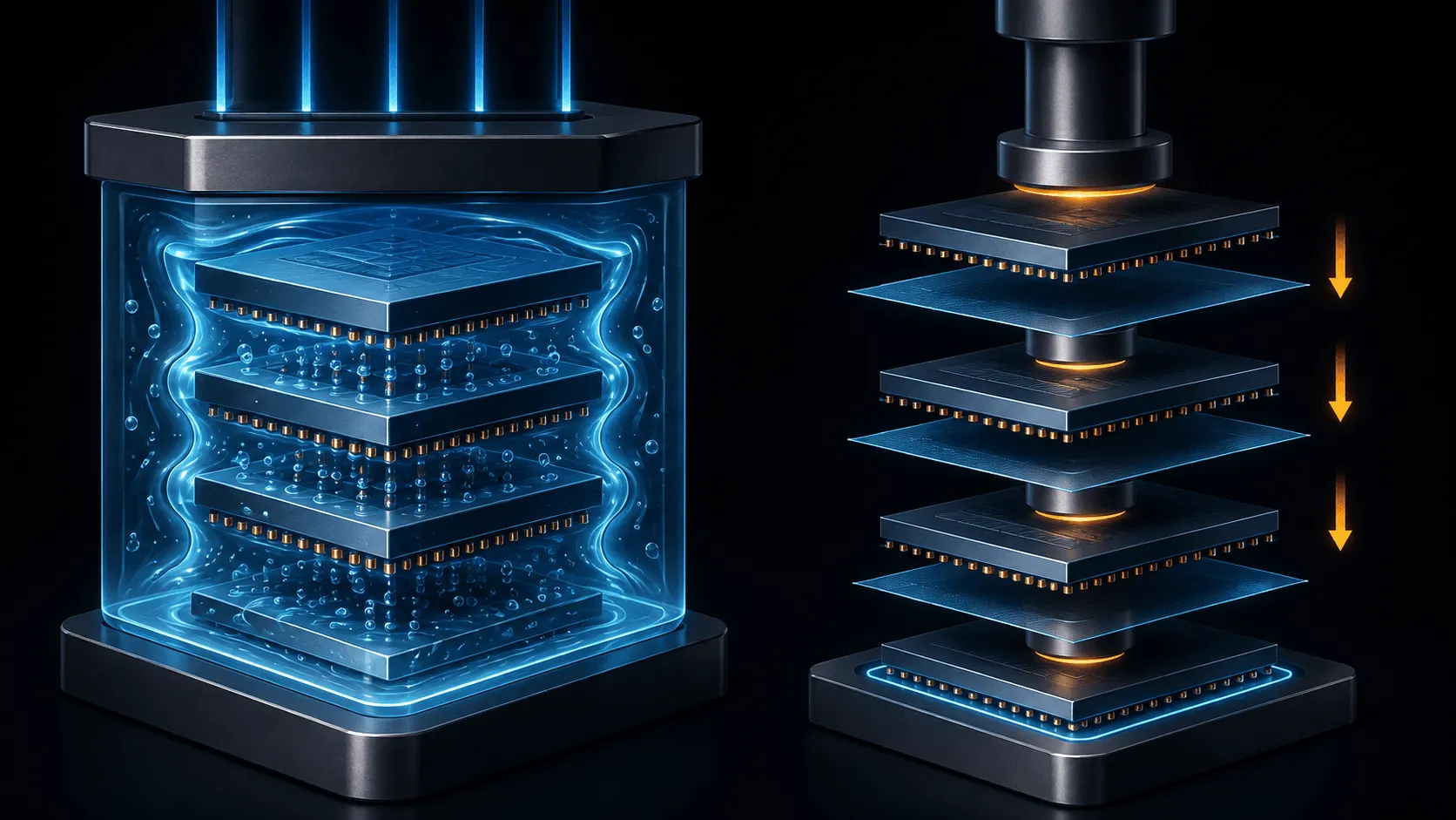
Current bonding methods fall into two main categories. SK hynix's "MR-MUF" stacks the dies first, then melts the solder all at once to bond them, before flowing a liquid protective material into the gaps and curing it—a method with fewer process steps and superior heat dissipation. Samsung's and Micron's "TC-NCF" sandwiches an insulating adhesive film (NCF) between dies and bonds them one layer at a time using heat and pressure. According to TrendForce, MR-MUF's protective material has roughly twice the thermal conductivity of NCF, and this difference has underpinned SK hynix's yield advantage.
HBM's high price stems not only from manufacturing difficulty but also from its structurally heavy wafer consumption. According to TrendForce's forecast, in 2026 HBM will account for 22% of DRAM wafer input, yet only 9% of total DRAM bit supply. Compared with the DRAM average overall, this works out to a simple calculation of roughly 2.4x (22% ÷ 9%) the wafer usage to produce the same capacity—and the gap widens further if compared only against ordinary DRAM. This is because TSVs and redundant circuitry expand die area, and defects compound through the stacking process. The more capacity manufacturers devote to HBM, the more tightly ordinary DRAM supply gets squeezed—and this is the structural origin of that dynamic.
What Changes with HBM4: 2,048-bit Widths and Logic-Based Base Dies Usher in the Custom Memory Era
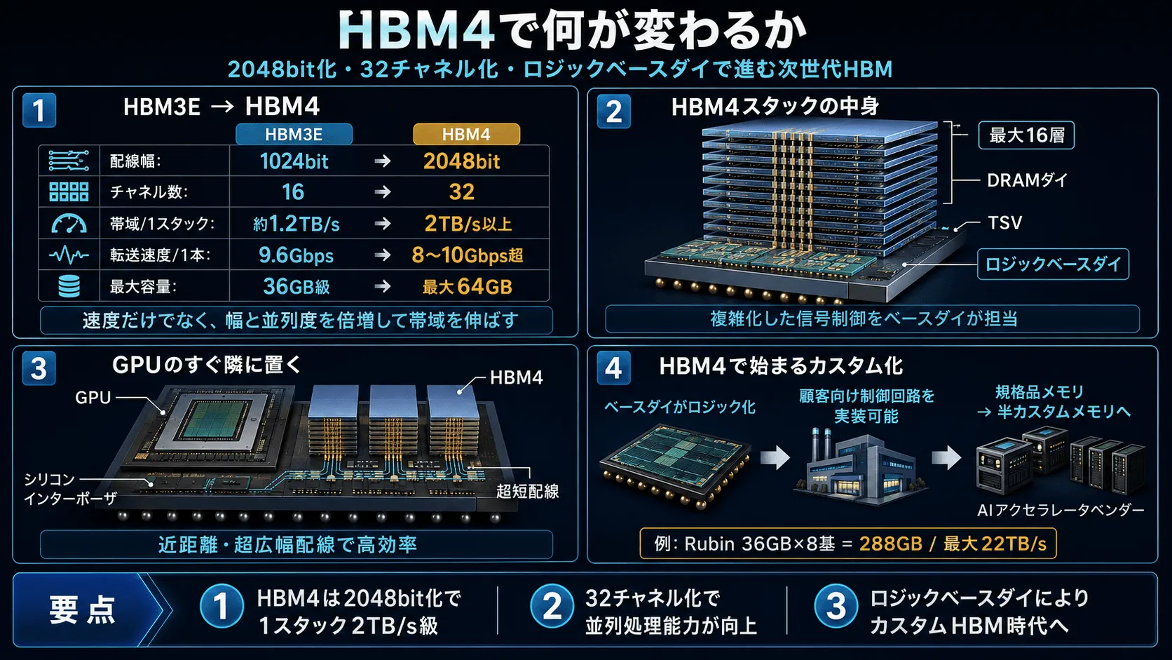
On April 16, 2025, JEDEC published the standard "JESD270-4," finalizing the shape of HBM4. The wire width per stack expands from 1,024 bits to 2,048 bits, and at a transfer speed of 8 Gbps, bandwidth reaches 2 TB/s. The number of channels doubles from 16 to 32, stacking is defined up to 16 layers, and capacity is specified up to a maximum of 64GB. This is a design that doubles width and parallelism simultaneously rather than pushing speed higher—an extension of the "gain bandwidth through width" approach that has defined HBM since HBM1.
| Generation | Primary Mass-Production Period | Speed per Wire | Bandwidth (per Stack) |
|---|---|---|---|
| HBM1 | 2015 | 1Gbps | 128GB/s |
| HBM2 | 2016– | 2.0–2.4Gbps | 256–307GB/s |
| HBM2E | 2020– | 3.6Gbps | 460GB/s |
| HBM3 | 2022– | 6.4Gbps | 819GB/s |
| HBM3E | 2024– | 9.6Gbps | approx. 1.2TB/s |
| HBM4 | 2026– | over 8–10Gbps | over 2TB/s |
SK hynix was first to develop the technology. The company began sample shipments of a 12-layer, 36GB product in March 2025, and on September 12 of that year announced what it called the world's first completion of HBM4 development and readiness for mass production. It claims an operating speed exceeding 10 Gbps—above the JEDEC standard's 8 Gbps—and a power efficiency improvement of over 40% compared to the previous generation, and unveiled a 16-layer, 48GB product at CES 2026.
Samsung, on the other hand, secured the lead in commercial shipments. On February 12, 2026, the company announced what it called the industry's first mass production and shipment to customers of commercial HBM4, touting an operating speed of 11.7 Gbps—about 46% above the JEDEC standard. Micron also announced on March 16, 2026 the start of mass shipments of a 12-layer, 36GB product (over 11 Gbps) destined for NVIDIA's next-generation GPUs, signaling that the competitive landscape is shifting from SK hynix's dominance through the HBM3E generation toward a more contested field.
In conventional HBM, even the bottom-layer base die was manufactured using the same process as DRAM. In HBM4, however, the circuitry required to control signals across 2,048 bits became too complex to fit within a DRAM process, so the base die has been replaced with a logic semiconductor. SK hynix entrusted this manufacturing to foundry leader TSMC's 12nm process, establishing the first-ever division of labor in which a memory-only manufacturer outsources logic production externally. Samsung, by contrast, manufactures its logic die in-house using its own foundry's 4nm process, positioning its integrated approach—from its most advanced 1c-generation DRAM process through to packaging, all done in-house—as its point of differentiation.
Once the base die becomes a logic semiconductor, control circuitry and features tailored to a customer's specific AI chip can be built directly into the memory itself. In other words, HBM4 also marks the gateway through which memory shifts from a "standard product" to a "custom product," with fully custom HBM tailored to individual customers expected to take hold in earnest with the next-generation HBM4E. Examples of this are already emerging: the GPU "Rubin," whose mass production NVIDIA declared at CES 2026, packs eight 36GB HBM4 stacks for a total of 288GB, with memory bandwidth reaching up to 22 TB/s—roughly 2.8 times the previous generation Blackwell's 8 TB/s. This is a design built with trillion-parameter-class AI models in mind, and GPU generational transitions are now completely synchronized with HBM generational transitions.
Leader SK hynix's Share Falls from 69% to 58% in a Year, as an Expanding Market Even Moves PC Memory Prices
According to market research firm Counterpoint Research, in Q1 2026 SK hynix led HBM revenue share with 58%, followed by Samsung and Micron tied at 21% each. A year earlier, in the same quarter, SK hynix's share stood at 69%. With Samsung mounting a comeback after falling behind in HBM3E, and Micron—a late entrant—rapidly gaining ground, what was once a runaway market is shifting into a genuine three-way contest.
Research firm Yole Group forecasts that HBM revenue will grow roughly 70% in a single year, from about $35 billion in 2025 to about $60 billion in 2026 (roughly ¥9 trillion at ¥150 to the dollar). By 2031, the figure is expected to reach approximately $170 billion—transforming what was once merely a subcategory of DRAM into one of the semiconductor industry's largest markets. The driving force is AI data centers: TrendForce expects per-chip HBM capacity in AI-focused ASICs (application-specific integrated circuits) to rise in 2026 from 96–192GB to 216–288GB.
As noted earlier, HBM consumes more than twice the wafer capacity for the same output as ordinary DRAM, and as all three companies have tilted production toward HBM, ordinary DRAM—which has nothing to do with AI—has fallen into a global shortage. According to TrendForce, DRAM industry revenue in Q1 2026 reached $97 billion, an 81% quarter-over-quarter increase driven by a sharp spike in contract prices, and some reports indicate that retail prices for PC-oriented DDR5 more than doubled in under a year. The direct cause behind rising prices for DIY PC memory and laptop memory upgrades in Japan is AI data center investment happening on the other side of the ocean.
TrendForce notes that in Q1 2026, per-wafer revenue for server DDR5 memory modules—specifically 64GB RDIMM (Registered DIMM) products—actually surpassed that of HBM. This reversal occurred because the price surge in ordinary DRAM was so sudden, temporarily upending the premise that "HBM is the highest-margin form of DRAM." The firm anticipates that, after a tug-of-war over supply allocation, HBM contract prices in 2027 could rise several-fold. Memory procurement costs have become a variable that determines the profitability of AI infrastructure construction itself.
The Main Battlefield Shifts to Back-End Processes: Japanese Companies Gain Ground in Equipment and Materials, and Micron Hiroshima's ¥1.5 Trillion Investment
No Japanese company manufactures HBM directly, but as the main competitive battlefield has shifted to the back-end "stacking" process, Japanese firms strong in equipment and materials are gaining greater prominence. In wafer-grinding equipment that thins wafers down to 30μm, Disco is a leading supplier; in wafer-bonding equipment, Tokyo Electron; in memory testers used for pre-shipment inspection, Advantest; and in molding equipment used for MR-MUF encapsulation, TOWA. On the materials side, Resonac supplies the insulating adhesive film NCF that is central to the TC-NCF method, while Ibiden is a major supplier of the package substrates that carry GPUs and HBM.
Micron held a groundbreaking ceremony on July 4, 2026, for a new fabrication building at its Hiroshima plant. The total investment is ¥1.5 trillion, with Japan's Ministry of Economy, Trade and Industry providing subsidies of up to approximately ¥500 billion, and equipment installation is scheduled to begin in the latter half of 2028. Hiroshima, Japan's only DRAM manufacturing site, is already mass-producing DRAM using the company's most advanced 1γ (one-gamma) generation process—and following equipment and materials, Japan is now also being incorporated into the next-generation HBM supply chain on the manufacturing side as well.
Three focal points lie ahead. The first is HBM4E and customization, which will take full shape in 2027; SK hynix is reportedly considering adopting TSMC's 3nm process for its logic die, while Samsung appears poised to respond with its own 4nm process—reshaping the alliance map between memory makers and foundries. The second is 16-layer bonding technology: Samsung has invested early in hybrid bonding, which directly joins dies together, though its yield is reportedly only around 10%, while SK hynix maintains its policy of tackling 16 layers using its proven MR-MUF method. The third is price: if the contract price surge that TrendForce projects for 2027 materializes, it will rewrite the very profitability calculus of AI investment itself.
The next time you come across an announcement of a new AI chip, look at the memory specifications before the compute performance figures. The HBM generation, capacity, and bandwidth it carries encapsulate both the performance that chip can actually deliver and the outcome of a procurement battle that has been playing out behind the scenes. A convenient touchstone will be the Rubin-equipped cloud offerings set to launch in the latter half of 2026, where the first measurable question will be how 22 TB/s of bandwidth changes the inference cost of trillion-parameter-class models.