


A Weibo post has sparked speculation about the internal layout of what's claimed to be Apple's next-generation SoC, the "A20 Pro." On August 30, a user known as 白饭炒白米饭 (Bairan Chao Baimifan) cross-referenced a diagram of solder pad placements with known chip configurations, estimating that the CPU would have 2 performance cores and 4 efficiency cores, while the GPU would have 7 cores. On top of that, theories about a 96-bit memory interface and a design placing the chip and DRAM side by side have also emerged.
If the move to 7 GPU cores is real, it would mean more execution units than the A19 Pro. However, feeding the GPU enough texture and other data is just as important as adding compute units. Qualcomm and MediaTek have already published designs that place data closer to the GPU to reduce transfers to external memory. The significance of this rumor becomes clearer when weighed against these rivals' approaches.
A 7-Core GPU Estimated from Solder Pad Layout
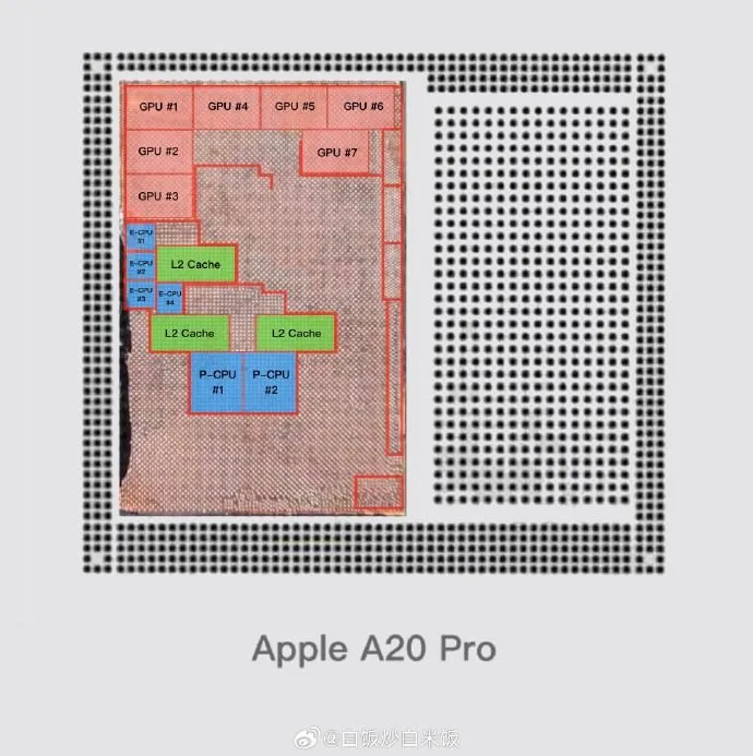
Apple's current A19 Pro, as officially described by the company, features a 6-core CPU and a 6-core GPU. In its explanation for the iPhone 17 Pro and Pro Max, Apple states that each GPU core incorporates Neural Accelerators, that GPU cache capacity has been increased, and that the chip works in tandem with a 16-core Neural Engine. In this design, the GPU isn't solely responsible for rendering—it's also tied into on-device AI processing.
This 7-core theory wasn't derived by directly counting cores from a die shot of the GPU. Rather, the poster tested 6-, 7-, and 8-core configurations against the assumed solder pad layout and concluded that 7 cores fit best. The original post has not been independently verified, and the authenticity of the image itself remains unconfirmed. This is not a configuration Apple has acknowledged.
If the core count does rise from 6 to 7 as in the A19 Pro, that would represent an increase of roughly 16.7% ((7÷6−1)×100). However, the makeup of the execution units and their clock speeds remain unknown, as do the power and cooling conditions. This does not mean GPU performance itself would improve by 16.7%.
| Item | A19 Pro (Apple's official specs) | This speculation regarding A20 Pro |
|---|---|---|
| CPU configuration | 6 cores | Estimated 2 performance + 4 efficiency cores |
| GPU configuration | 6 cores | Estimated 7 cores |
| GPU/AI description | Neural Accelerators in each GPU core, increased cache, coordination with 16-core Neural Engine | Not yet confirmed |
| Memory spec/bus width | Not mentioned in the Apple materials referenced | 96-bit theory circulating; whether it's LPDDR5X or LPDDR6 is unconfirmed |
| Performance claims | Up to 40% improved sustained performance vs. previous-generation iPhone, combined with vapor chamber | No measured figures exist for this speculation |
The idea of adding one more GPU core is really about how far Apple might expand its computing resources for both rendering and AI workloads. The "up to 40%" figure in the table refers to a comparison of sustained device performance including cooling—a different metric entirely from the rate of increase in GPU core count.
How Would a 96-bit Bus Change Data Supply?
The number 96-bit doesn't directly indicate computational performance. Theoretical memory bandwidth is calculated by multiplying per-pin transfer speed by bus width, then dividing by 8 to convert from bits to bytes. So, assuming the same transfer speed, going from 64-bit to 96-bit would be a 1.5x increase (96÷64), boosting theoretical bandwidth by 50%. This 64-bit figure isn't a confirmed spec for the A19 Pro or any competing chip—it's simply a comparison model illustrating the effect of width alone.
Increased bandwidth could speed up workloads that are bottlenecked by memory transfer wait times. In scenarios like high-resolution game rendering, image processing, and on-device AI all accessing the same main memory, simply speeding up the GPU alone wouldn't resolve resource contention. On the other hand, for workloads where compute capability or heat dissipation is the limiting factor first, boosting bandwidth wouldn't yield proportional performance gains. You can't predict game frame rates from a 50% increase in bus width alone.
Rumors about changing how memory is connected also touch on packaging design. TSMC's InFO_PoP is a technology that stacks DRAM packages onto mobile processors, connecting them through redistribution layers and through-silicon vias. In contrast, there's a theory that the A20 Pro uses a package called WMCM, which places memory side by side with the chip instead. However, Apple has not confirmed adopting this.
While side-by-side placement could open up more wiring options, bus width is ultimately determined together with the memory controller and other design elements. You can't derive a 96-bit bus or a 7-core GPU just from the name of a packaging method. The continuation of LPDDR5X also hasn't been confirmed—memory spec changes, bus width expansion, and packaging changes all need to be verified independently.
How Snapdragon and Dimensity Reduce Memory Transfers
Qualcomm's Snapdragon 8 Elite Gen 5 features a dedicated 18MB HPM for the Adreno GPU, along with a Tile Memory Heap that optimizes memory usage and bandwidth. MediaTek, meanwhile, describes a Dimensity Dynamic Cache Architecture for the Dimensity 9500, listing 16MB of L3 cache and 10MB of SLC in its specs. Apple also claims to have increased GPU cache in the A19 Pro, but the capacity isn't specified in the announcement referenced here.
| SoC | How the GPU is disclosed | Cache/memory transfer measures | Main memory specs disclosed | Performance comparison conditions |
|---|---|---|---|---|
| Apple A19 Pro | 6-core GPU | Increased GPU cache; Neural Accelerators in each GPU core | Spec/bus width not disclosed in materials | Up to 40% improved sustained performance vs. previous-generation iPhone, including cooling |
| Snapdragon 8 Elite Gen 5 | Adreno; no comparable core count disclosed in referenced materials | Dedicated 18MB HPM for GPU, Tile Memory Heap | LPDDR5x supported | Qualcomm's claim of 23% GPU performance improvement vs. Snapdragon 8 Elite |
| Dimensity 9500 | Arm Mali-G1 Ultra MC12 | Dynamic Cache Architecture, 16MB L3, 10MB SLC | LPDDR5X supported | MediaTek's claim of 33% peak performance improvement vs. previous-generation Dimensity flagship |
A GPU-dedicated 18MB and a CPU's L3 or chip-wide SLC can't be compared on capacity alone. Qualcomm explicitly labels its 18MB as a GPU-dedicated HPM, while MediaTek's 16MB L3 and 10MB SLC are presented as specs that include the CPU hierarchy—meaning these numbers don't represent the same kind of resource as the dedicated 18MB. Apple, too, only states that it has "increased GPU cache" without disclosing a figure. How effective a cache is depends not just on its size but on who can access it and which processes it helps avoid sending to external memory.
Qualcomm's Tile Memory Heap is a mechanism for making nearby Adreno memory easier to use, reducing transfers to external memory. MediaTek's dynamic cache is similarly presented as a mechanism for making GPU memory usage more efficient. Neither improvement can be explained by external memory transfer speed alone.
If a wider bus is confirmed for the A20 Pro, it would allow more data to be moved at once even at the same memory speed. The cache and memory-optimization techniques that rivals emphasize, meanwhile, reduce the amount of data that needs to be moved in the first place. Since the two approaches can be combined, any changes to Apple's bus width should be considered alongside potential changes to GPU cache.
Sustained Performance Worth Verifying After the Announcement
Qualcomm's 23% figure and MediaTek's 33% figure are both manufacturer-reported numbers benchmarked against their own previous generations. Without matching comparison chips, devices, and test conditions, these figures alone can't be used to rank Snapdragon against Dimensity—let alone against the unreleased A20 Pro. The Mali-G1 Ultra's MC12 configuration also isn't measured in the same compute-unit terms as Apple's rumored 7-core GPU.
Apple states that pairing the A19 Pro with a vapor chamber delivers up to 40% better sustained performance than the previous generation. In scenarios like extended gaming sessions or continuous on-device AI use, what matters is how well performance holds up once heat builds up. Even if wider bandwidth is confirmed, its real-world impact can't be determined without also considering the device's heat dissipation, memory controller, and how the OS and apps allocate resources.
Apple has announced a special event for September 9 at 10 a.m. Pacific Time (2 a.m. JST on September 10), though it hasn't disclosed any product names or specifications. Once the official GPU configuration is known, frame rates and power consumption during sustained gameplay at identical image quality will serve as useful benchmarks. For AI workloads, it will be worth checking—under the same model and processing conditions—whether memory transfer is a limiting factor on performance. If the added compute units and improved data supply align well with the thermal design, short bursts of speed could translate into performance that holds up over time.