

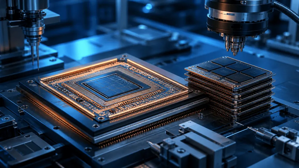
Applied Materials said on August 13 that it expects 2026 advanced packaging revenue to grow more than 70% year-over-year. Since its May forecast called for growth of more than 50%, the company raised the lower bound of its growth guidance by 20 percentage points in just three months. Investment in AI semiconductors is flowing not only into front-end miniaturization but also into HBM (High Bandwidth Memory) and 3D packaging that connects multiple dies, expanding the very range of processes where the company can sell equipment. Revenue for the May-July 2026 quarter reached an all-time high of $9,115 million.
Over 70%: A 20-Point Upward Revision in Three Months
Revenue for the May-July quarter rose 25% year-over-year and roughly 15% quarter-over-quarter. CEO Gary Dickerson explained that the sequential increase from the prior quarter was the largest in the company's history. Revenue from Semiconductor Systems, the semiconductor manufacturing equipment segment, was $7,040 million, up 27% from $5,564 million in the same quarter a year earlier.
For the August-October quarter, the company forecasts revenue of $10,250 million plus or minus $500 million, and non-GAAP earnings per share of $4.02 plus or minus $0.20. The midpoint of the revenue guidance is about 12.5% above the May-July quarter. Applied Materials defines calendar year 2026 as running from the second quarter of fiscal 2026 through the first quarter of fiscal 2027, with the final quarter including 14 weeks—one more than usual.
Advanced packaging is not an independent accounting segment. Because its revenue is included in both Foundry/Logic and DRAM, the absolute dollar amount cannot be calculated from the over-70% figure alone. Even so, the upward revision from May's over-50% figure shows how quickly the center of gravity for AI-related equipment investment is spreading from on-chip processing to the processes that densely connect multiple chips.
HBM Stacking Extends Equipment Demand into Back-End Processes
HBM is built by stacking thinly ground DRAM dies and connecting them via TSVs (Through-Silicon Vias) and fine copper wiring. As the number of stacked layers increases, surface flatness, connection height, die warpage, and microscopic defects all become critical to yield. Because a single defect can ruin an entire stack, packaging processes now require measurement and inspection precision approaching that of front-end wafer processing.
The six products Applied Materials announced in June span this entire process. The Opta Quad CMP handles the surface planarization required for hybrid bonding, while the Nokota VMax 2 ECD ensures uniform copper plating for TSVs and microbumps. The Producer Avila 2 PECVD suppresses warpage in thin DRAM dies for 12- and 16-layer HBM. In addition, the VeritySEM 7AP measures dimensions with sub-10nm sensitivity, and the SEMVision G7AP uses electron beams to classify defects that are difficult to detect optically.
This expanding range of equipment changes what the over-70% growth figure actually means. The source of demand isn't limited to a single type of bonding tool. Multiple processing tools—for deposition, polishing, and plating—are required, along with measurement and defect review. Applied Materials is transferring its existing front-end technologies into packaging, aiming to capture the ramp-up in HBM and 3D packaging across multiple product lines.
Revenue opportunities in packaging equipment also diverge based on the dimensions and substrate types that can be processed. The VeritySEM 7AP measures the thick, warped substrates used in HBM and chiplets. The SEMVision G7AP classifies defects across silicon, organic materials, and glass, and has already entered volume production at major memory and logic manufacturers. The over-70% outlook is not based solely on these newly announced products.
Reading the 26% DRAM Share
DRAM's share of Semiconductor Systems revenue was 26% in the May-July quarter, down 3 points from 29% in the February-April quarter. However, total revenue for the segment grew 18%, from $5,965 million in the prior quarter to $7,040 million. The decline in DRAM's share doesn't mean DRAM revenue fell—rather, the overall base, which includes Foundry/Logic and flash, expanded even faster.
In May, the company had stated that DRAM revenue was $1.7 billion, up 18% year-over-year. In its August earnings call, it said it expects strong revenue growth in the second half of the calendar year across DRAM, advanced Foundry/Logic, and advanced packaging. In HBM, both the equipment used to manufacture DRAM dies and the equipment used to stack and inspect them benefit from the same investment cycle.
The constraint on capacity expansion is cleanroom space at customer fabs. In its May earnings call, the company explained that increased delivery requests for 2026 stemmed from customers reallocating existing space and adding new space. The new Centura Prime Epi reduces footprint by 20% compared to the previous model. Shrinking equipment size is itself a way to increase DRAM output from limited floor space.
China at 28%: Declining Share, Steady Revenue
China remained Applied Materials' largest revenue region in the May-July quarter, accounting for 28% of total company revenue, or $2,506 million. While this share fell 7 points from 35% in the same quarter a year earlier, revenue itself declined only about 1.6%, from $2,548 million. Rather than a sharp contraction in China business, the decline in China's share of the total reflects strong growth in regions outside China.
Compared to the previous quarter, China's revenue rose from $2,087 million, and its share also rose 1 point from 27%. Taiwan accounted for 22%, South Korea 17%, and the United States 15%. While concentration in China has eased somewhat compared to a year earlier, it remains at a scale significant enough to influence the growth of equipment makers.
As of May, Applied Materials expected its China business and global ICAPS business to be roughly flat to slightly up for the calendar year. By August, it forecast growth in both China and ICAPS for both 2026 and 2027. ICAPS refers to IoT and communications applications, along with mature and specialty processes for automotive, power, and sensor applications—capital investments distinct from cutting-edge AI products.
Whether the over-70% packaging growth forecast translates into actual results will first be tested by whether August-October quarter revenue reaches around $10,250 million. Beyond that, growth in 2027 will hinge on how much customers expand their cleanrooms and continue placing orders for HBM and 3D packaging equipment.