


On August 24, Arm disclosed the internal architecture of its data-center-focused "Arm AGI CPU" at Hot Chips 2026. Arm's presentation slides revealed that, beyond the 136-core, 300W specifications shown at the product's March launch, the chip uses two compute chiplets, each containing 70 cores. Each chiplet carries over 50 billion transistors, bringing the total to more than 100 billion. What this disclosure reveals is a design philosophy: rather than building one massive die, Arm links two identical chiplets—each equipped with its own memory and I/O—via a high-speed interconnect to maximize CPU density within a rack.
Two Chiplets of 70 Cores Each, 136 Cores in the Product
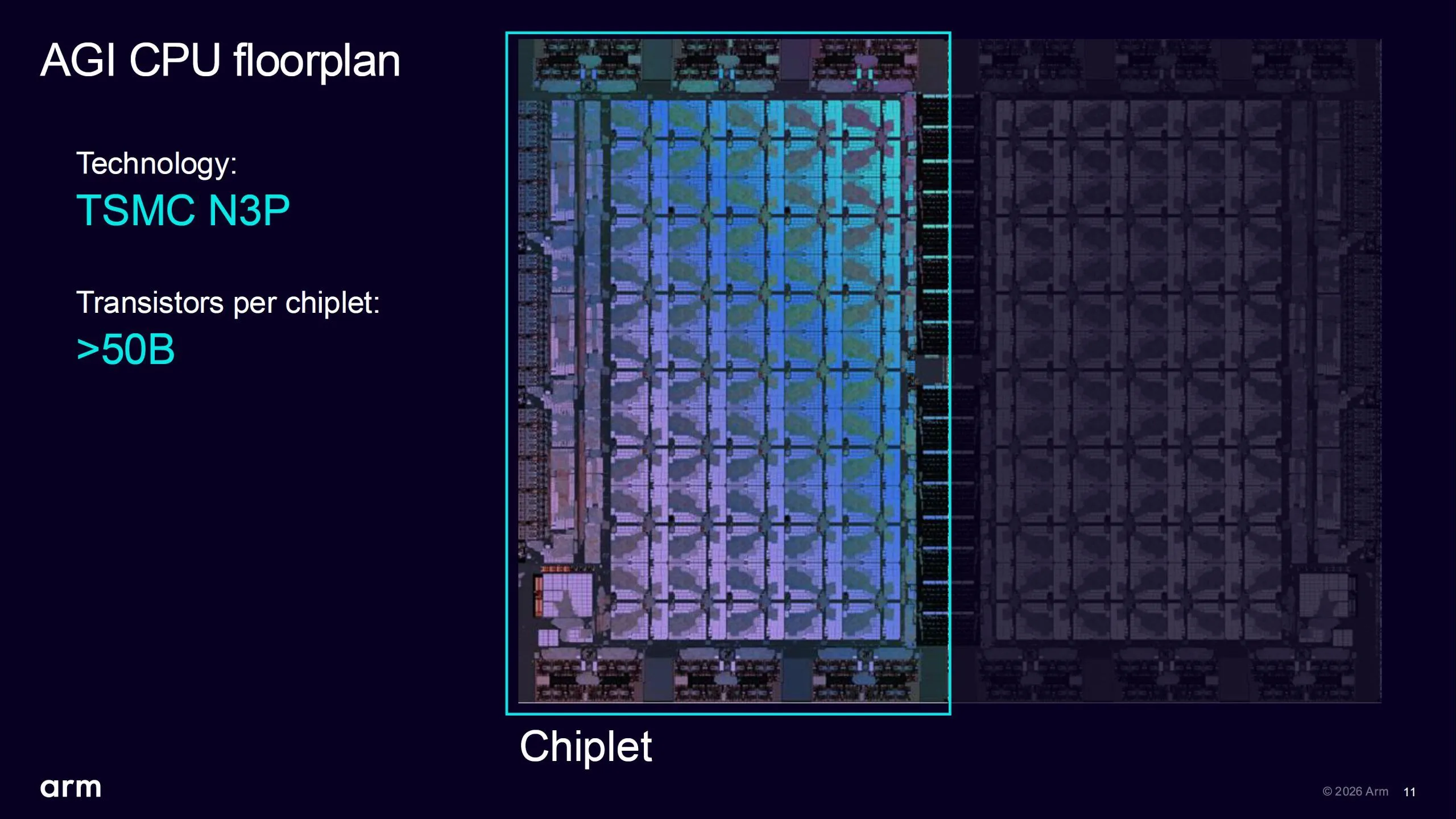
The AGI CPU consists of two compute chiplets fabricated on TSMC's N3P process. Each chiplet contains 70 Neoverse V3 cores, each paired with a 64KB instruction cache, a 64KB data cache, and a dedicated 2MB L2 cache per core. Together, the two chiplets physically house 140 cores, but the top-end SKU enables only 136 of them. Arm has not explained why the remaining four cores go unused.
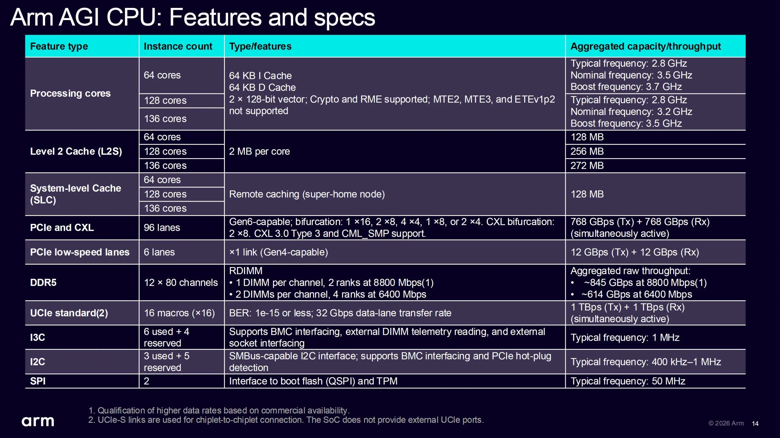
The shared cache figures require careful reading as well. The 136-core version has 272MB of dedicated per-core L2 cache in total, but its system-level cache (SLC) is 128MB. Notably, the SLC capacity stays the same across all SKUs—64, 128, and 136 cores. Only the L2 cache scales with core count; SLC capacity does not increase on a per-core basis.
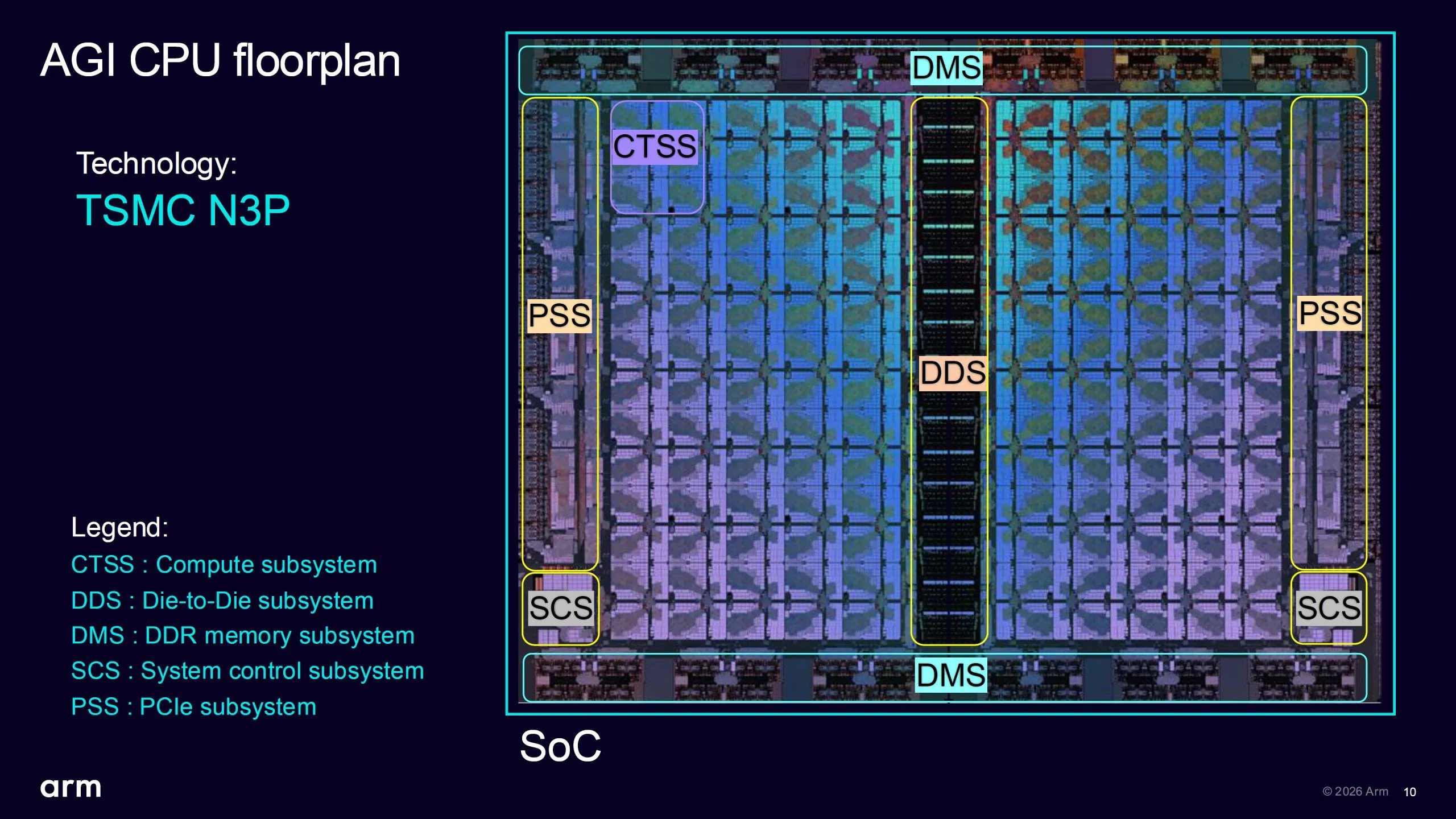
Each chiplet integrates not just the CPU cores but also DDR memory and PCIe subsystems, along with system control logic and chiplet-to-chiplet communication circuitry. There is no separate dedicated I/O die; instead, the two chiplets mirror each other in structure. The floorplan—with memory controllers positioned at the top and bottom of the die, PCIe on the outer edges, and the inter-chiplet link circuitry toward the center—illustrates a design that splits not just compute, but also data routing, into two symmetric halves.
Power and thermal management are also finely controlled at the chiplet level. Local power management for each core row uses a Cortex-M55, while system control for each chiplet is handled by a Cortex-M7. Voltage rails are also shared on a per-chiplet basis, allowing hierarchical coordination of both chiplets' operation within the 300W power envelope.
UCIe's Role in Connecting Over 100 Billion Transistors
The two chiplets maintain cache coherency through a UCIe-S compliant link. Each chiplet has 16 x16 macros operating at 32Gbps per lane. The aggregate bandwidth is 1Tbps in each direction, transmit and receive, usable simultaneously. However, this UCIe interconnect is strictly for intra-package use—it is not a port for adding external chiplets.
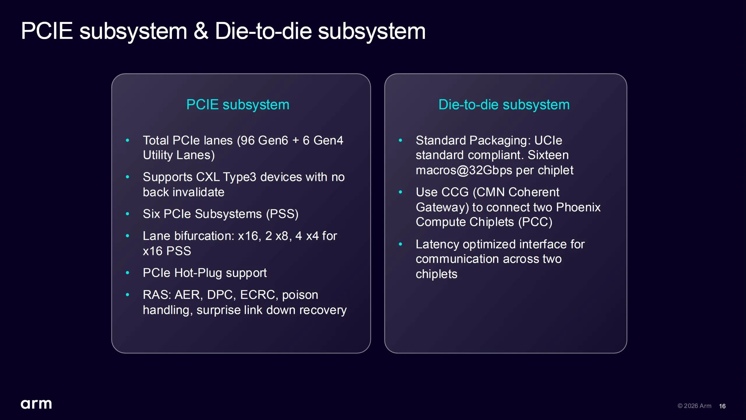
For external accelerators and memory expansion, the chip uses 96 lanes of PCIe Gen6 and CXL 3.0 Type 3. The aggregate PCIe bandwidth is 768GB/s in each direction, transmit and receive, plus a separate 6-lane Gen4 utility link. As a host CPU that hands work off to GPUs or NPUs and receives results back, adding more compute cores alone doesn't help if I/O becomes a bottleneck and leaves accelerators waiting. The AGI CPU devotes as much silicon area to pathways—both within and beyond the package—as it does to core count.
Memory is configured as twelve 80-bit DDR5 channels. In a 1 DIMM-per-channel configuration, it supports DDR5-8800, yielding a theoretical raw bandwidth of approximately 845GB/s. A 2 DIMM configuration runs at DDR5-6400, delivering about 614GB/s. The speed Hot Chips materials described as validated for mass production is DDR5-8000; certification up to 8800MT/s depends on the availability of commercial memory modules. There remains a gap between the product's stated upper limit and its validated status for mass production.
A CPU Built to Keep AI Running, Not a GPU
The name "AGI" might suggest an AI compute engine, but the Neoverse V3 is a general-purpose server CPU core based on Armv9.2. The heavy matrix operations of large models are primarily offloaded to GPUs or NPUs, while the CPU handles agent scheduling, tool calls, and pre/post-processing for inference. Managing memory and I/O, and running multiple processes in parallel, also falls to the CPU side.
The core's internal architecture, as presented at Hot Chips, aligns with this role. The front end is 10-wide, with an out-of-order execution window exceeding 384 entries—instructions are dispatched 10-wide and retired 8-wide. The integer side features 8 ALUs and three branch-processing pipelines, with enhanced branch prediction and data prefetching. For control-flow-heavy code where the type of processing changes frequently, minimizing missed branches and memory stalls matters more than peak matrix-multiplication throughput.
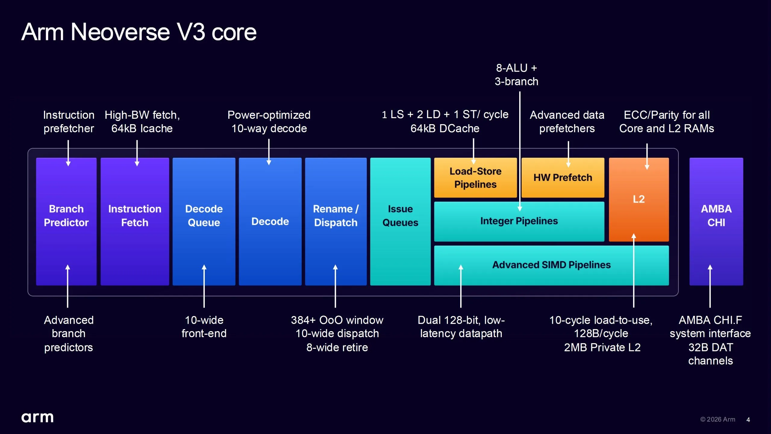
On the AI-oriented side, dual 128-bit SVE2 pipelines handle bfloat16 and INT8 instructions. Still, the design's focus is not vector width alone. It combines a 2MB L2 cache with a 10-cycle data transfer latency, 128 bytes-per-cycle of L2 bandwidth, and over 6GB/s of memory bandwidth per core—aimed at pushing through large volumes of small, irregular CPU-side workloads.
Three SKUs Trade Off Core Count Against Memory Headroom
Arm's presentation slides broke down three SKUs by typical, base, and boost frequencies. While the 300W baseline TDP and 128MB SLC are shared across all three, reducing core count increases the memory bandwidth available per core.
| SKU | Active Cores | Frequency (Typical / Base / Boost) | Total L2 | Memory Bandwidth per Core |
|---|---|---|---|---|
| Max Core Count | 136 | 2.8 / 3.2 / 3.5GHz | 272MB | 6GB/s |
| TCO-Optimized | 128 | 2.8 / 3.2 / 3.5GHz | 256MB | 6.3GB/s |
| Max Memory per Core | 64 | 2.8 / 3.5 / 3.7GHz | 128MB | 13GB/s |
The 136-core version maximizes parallelism, while the 64-core version divides the same 12 memory channels among less than half the cores, pushing per-core bandwidth to 13GB/s. This makes the 64-core version less a budget option and more a deliberate choice for workloads like databases and analytics, where memory supply matters more than core count. Arm's decision to place SKUs with different core counts at the same 300W isn't about establishing a power hierarchy—it's about letting customers choose, within a fixed power budget, whether to prioritize parallelism or per-core resources.
$2 Billion in Demand Doesn't Mean Confirmed Sales
The product's rollout requires distinguishing between expressions of demand and actual production status. On July 29, Arm stated that customer demand across fiscal years 2027 and 2028 combined had surpassed $2 billion. The company has already shipped early units to multiple customers, but SEC filings as of the end of June indicate that full-scale production is planned by the end of 2026. Shipping early units and ramping up mass production are not the same stage.
Manufacturing capacity for the full $2 billion in demand has also not been fully secured. What Arm has confirmed as secured is the manufacturing capacity to support a previously disclosed $1 billion opportunity; the company is working with manufacturing and supply chain partners to expand capacity to meet the remaining demand. Furthermore, "demand" is not synonymous with recognized revenue or confirmed shipment volume. Arm itself acknowledges that selling complete CPUs may differ from its traditional IP licensing business in terms of margins, revenue recognition, and sales cycles.
The claim that the same 36kW rack delivers more than double the performance of the latest x86 systems is also, at this point, Arm's own estimate. One can calculate that packing 30 blades, each with two 136-core CPUs, yields 8,160 cores of density. But actual application performance, sustained operation at 300W, and sub-100ns memory latency must still await third-party measurement. Only once mass production begins by the end of 2026 and these figures are reproduced on customer systems will the design investment behind more than 100 billion transistors translate into real-world rack workloads.