

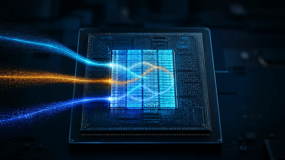
BTQ Technologies and Taiwan's Industrial Technology Research Institute (ITRI) announced on August 7, 2026, that they had verified the core IP for "Quantum Compute-in-Memory (QCIM)," which processes post-quantum cryptography, in TSMC's 28nm design environment. They stated that they executed cryptographic processing related to FIPS 203, 204, and 205, standardized by the U.S. National Institute of Standards and Technology (NIST), confirming functional correctness and design feasibility. In the implementation race following the finalization of the standards, this represents a step forward in the path toward loading both key encapsulation and different types of digital signature schemes onto a single reconfigurable accelerator.
However, this achievement is not a measurement report of a completed 28nm chip. What BTQ has disclosed is verification of the core in a design environment, and figures for speed, power consumption, and circuit area have not been released. The value of QCIM will be determined by whether its design advantages can be translated into measured values during the upcoming module integration and prototype chip stages.
Processing Scope Confirmed in the 28nm Design Environment
What was completed this time is the first technical milestone in a multi-year plan being pursued by BTQ and ITRI. In January 2026, the two companies had announced plans to evaluate the feasibility, performance, and energy efficiency of QCIM at the silicon level and to create benchmarks usable for product design. In the August announcement, they explained that they ran the core IP in a design environment for TSMC's 28nm process and confirmed the functional correctness of cryptographic processing under multiple operating conditions.
FIPS 203, 204, and 205, which were subject to this verification, are the first three post-quantum cryptography standards approved by NIST in August 2024. The three standards do not redundantly cover the same task.
| Standard | Algorithm | Primary Role |
|---|---|---|
| FIPS 203 | ML-KEM | Key encapsulation to establish a shared key over a public channel |
| FIPS 204 | ML-DSA | Digital signature based on module lattices |
| FIPS 205 | SLH-DSA | Stateless digital signature based on hash functions |
FIPS 203 and 204 use lattice problems, while FIPS 205 is based on hash functions. The result that QCIM executed processing related to all three standards demonstrates that a design aiming for broader processing scope than a circuit dedicated solely to one type of lattice cryptography has—at least within the verification environment—proven viable. However, NIST has not certified QCIM, and no test results demonstrating full compliance with the standards have been published.
A Design That Shifts Computation Toward Memory
QCIM is not the name of a finished chip but rather the design of a cryptographic accelerator provided as synthesizable soft IP. BTQ is responsible for the cryptographic architecture. South Korea's ICTK contributes secure semiconductor and physically unclonable function (PUF) technology. ITRI handles semiconductor design, integration, and verification. The aim is a configuration that can be embedded into ASICs or FPGAs depending on the application and ported across different manufacturing processes.
At its core is the concept of performing cryptographic operations within the memory subsystem. A typical processor reads data from memory, processes it in a computation unit, and writes the result back to memory. BTQ explains that for the large volumes of working data handled by post-quantum cryptography, this back-and-forth increases latency and power consumption. QCIM aims to reduce data transfer by performing many simple bitwise operations in parallel, close to memory.
Another goal is cryptographic agility. If a dedicated circuit is fixed to a single algorithm, responding to standard revisions or changes in adopted schemes requires hardware replacement. QCIM adopts a design that handles both conventional cryptography and multiple post-quantum cryptographic schemes within the same block by varying instructions and combinations of processing. This verification spanning FIPS 203 through 205 serves as the first piece of evidence confirming this reconfigurability.
However, flexibility and efficiency do not automatically go hand in hand. While fixed circuits designed for a narrow application can more easily achieve high performance, reconfigurable circuits impose additional burdens in terms of control and memory. For QCIM to enter mass production, it will need to demonstrate through actual measurements that the advantage of handling multiple schemes outweighs the increase in circuit area and power consumption.
Differences Between QCIM and Prior Chips
QCIM is not the first attempt to accelerate post-quantum cryptography in hardware. "Sapphire," announced by an MIT research team in 2019, was a configurable lattice-based cryptography processor actually fabricated using TSMC's 40nm low-power CMOS process. The cryptographic core fit within 0.28 square millimeters and used 106,000 logic gates and 40.25 kilobytes of SRAM to run algorithms such as Kyber and Dilithium, which were in NIST's second selection round at the time.
Sapphire made polynomial arithmetic and sampling for lattice-based cryptography efficient and demonstrated on actual silicon that post-quantum cryptography could be executed on low-power devices. Given this precedent, process node size alone—28nm in this case—cannot explain what is new about QCIM. The distinction QCIM puts forward lies in distributing a memory-centric computation approach as synthesizable IP and consolidating processing for the three standards finalized in 2024 into a single reconfigurable block.
Gaps still remain in any comparison. Sapphire disclosed chip area, gate count, and SRAM capacity, and measured performance and energy efficiency on actual silicon. BTQ, meanwhile, does list cycle counts and performance estimates on its QCIM product page, but has not disclosed measurement conditions or comparison targets as part of the August verification results. At this stage, the two cannot be numerically compared to determine superiority.
Performance Figures to Be Determined by the Next Prototype Chip
Development will next move to module-level integration, verification, and validation, incorporating the QCIM core into a larger system. This stage will examine not only the standalone functionality of the core but also whether processing performance and interoperability can be maintained once connected to peripheral circuits and interfaces. Based on the results, BTQ plans to make decisions regarding manufacturing, customer demonstrations, and application-specific product configurations.
BTQ has also indicated that it expects to ship prototype chips to key customers and strategic partners by the end of 2026 for performance and functionality evaluation. This is not a confirmed shipping date. The announcement lists this as contingent on the success of subsequent integration and verification, as well as on foundry supply capacity, customer requirements, and development resources.
What is needed at the prototype stage are not descriptive terms like "fast" or "low power consumption." What is needed are figures: at what operating frequency and voltage, how many cycles each FIPS process requires, and how many joules a single operation consumes. To expand adoption as IP, circuit area, required SRAM capacity, and countermeasures against side-channel attacks will also be essential. If these conditions are met in the year-end customer evaluations, QCIM will advance from a technology that has completed design verification to a semiconductor IP on which adoption decisions can be made.