

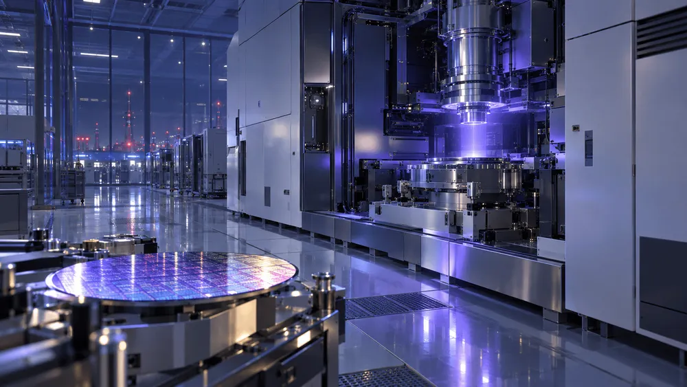
NVIDIA CEO Jensen Huang predicted on the All-In Podcast, released September 14, 2026, that China will "reach" advanced lithography equipment by 2030. According to remarks reported by Tom's Hardware, Huang cited China's mass-production capabilities and suggested that "two or three years is nothing." However, the published question and answer refer simply to "advanced lithography equipment" without specifying whether this means immersion deep ultraviolet (DUV) or extreme ultraviolet (EUV) lithography, or whether it refers to a prototype or a production-ready machine. To properly evaluate the 2030 timeline, we first need to clarify what "reaching" this milestone actually means.
What Does "Reaching" 2030 Actually Mean?
Lithography equipment development involves multiple stages, each representing a different kind of "success": generating EUV light, exposing circuit patterns on wafers, manufacturing identical-performance machines repeatedly, and achieving qualification on customers' production lines. The technical difficulty and business implications differ enormously between the first stage and the last.
Huang did not clearly distinguish between these stages in his remarks. Therefore, we cannot treat the prediction "a working EUV lithography prototype will exist by 2030" as equivalent to "China will have mass-production capacity comparable to ASML by 2030." The former could be satisfied by a single demonstration unit, while the latter requires supplying multiple units, ensuring stable operation, and providing ongoing maintenance support.
The speaker's position should also be considered. NVIDIA has business interests tied to both Chinese market access and U.S. semiconductor export policy. Huang's view represents a strategic long-term assessment of China's manufacturing capabilities—not a development roadmap presented by a lithography equipment manufacturer. This isn't grounds for dismissing the prediction, but neither is it grounds for treating it as a confirmed roadmap.
Immersion DUV and EUV Aren't Measured on the Same Scale
China's government procurement network announced on December 25, 2025, that it had procured one "SSC800/10" step-and-scan lithography system manufactured by Shanghai Micro Electronics Equipment (SMEE) for 109,999,850 yuan. This confirms that a commercial transaction for a domestically produced machine with a model number did take place. However, the announcement did not disclose resolution, overlay accuracy, throughput, or intended application—making it impossible to determine whether the equipment has performance suitable for advanced semiconductor mass production.
Shanghai's 2024 Key Technology Equipment Catalog set target specifications for 300mm-wafer-compatible ArF lithography systems: a 193nm light source wavelength, resolution of 65nm or better, and overlay accuracy of 8nm or better. These are policy-catalog target requirements, not measured values from an actual product. They cannot be equated with the SSC800/10's actual specifications or with the reported performance of China's domestically produced immersion DUV lithography systems.
Immersion DUV and EUV are not simply interchangeable technologies where one fully replaces the other. EUV enables complex layers in advanced chips to be formed with fewer exposure passes, while many layers in production processes still rely on immersion DUV. Even if China achieves domestic production of immersion DUV systems, EUV challenges remain; conversely, even if an EUV lithography prototype becomes operational, mass-production capacity for DUV lithography systems will continue to be necessary.
What China's Public Records Reveal About Accumulated Component Technologies
In a 2023 response, the Shanghai Municipal Science and Technology Commission explained that China launched national research projects related to EUV lithography in 2008, 2012, and 2018. These projects cover not only EUV light sources and projection optics but also magnetic levitation wafer stages, photoresists, and measurement technologies. Research platforms and patents have also been established, and public records indicate that China's efforts are not limited to light source technology alone.
However, this response does not demonstrate the existence of a complete EUV lithography system or any mass-production track record. Because 13.5nm-wavelength EUV light is absorbed by air and conventional lenses, the equipment's interior must be maintained in a vacuum, with light guided through multilayer reflective mirrors. Only when light sources, reflective optics, masks, and other processes are integrated—with wafer stages synchronized at high speed and high precision—does the system function as a complete lithography machine. Having research foundations in individual component technologies is a separate stage from completing an integrated commercial machine.
In December 2025, Reuters reported, based on multiple sources, that a prototype EUV lithography system at a classified facility in Shenzhen was completed earlier that year and successfully generated EUV light. However, the machine has not yet manufactured a functioning chip, and neither the equipment specifications nor third-party measurements have been publicly disclosed. While the Chinese government has set a goal of producing a working chip by 2028, sources close to the plan told Reuters that 2030 is considered more realistic. This 2030 figure refers specifically to the outlook for the first functioning chip—it does not indicate the start of mass production or the achievement of performance comparable to ASML.
From Prototype to Mass Production: What Remains Before 2030
ASML took approximately 10 years to progress from shipping its first EUV prototype in 2010 to shipping its 100th unit, passing through a production-model shipment in 2013. From the early-2025 completion of China's reported prototype to 2030 is roughly five years—meaning that if Huang's prediction refers to mass-production capacity, China would need to compress ASML's maturation process into roughly half the time. However, since China can draw on existing technical knowledge and talent, and since equipment performance targets may not be identical, this comparison alone cannot determine success or failure.
According to ASML's official history, the company shipped its first EUV prototype system, the NXE:3100, to a customer in 2010, and shipped its first EUV production system, the NXE:3300, in 2013. By early 2020, cumulative shipments had reached 100 units. ASML states that it invested over €6 billion in R&D over 17 years, and that developing EUV lithography technology as a whole took more than 20 years.
This timeline is not a benchmark for directly predicting when China will achieve completion. China has access to publicly available technical knowledge, and Reuters reported that former ASML engineers and secondhand components were also utilized in the project. On the other hand, ASML's 100th shipment and China's first functioning chip represent different stages of achievement. What this comparison does suggest is that if China intends to progress to mass-production capacity by 2030, it must complete equipment integration, ensure reproducibility, and achieve customer qualification—all within a compressed timeframe following EUV generation.
Resolution Alone Doesn't Determine Production-Grade Equipment
In 2025, ASML sold 48 EUV lithography systems and 279 immersion DUV lithography systems. The EUV production model NXE:3800E offers a full-configuration throughput of 220 wafers per hour, and existing installed units have been upgraded to the same level. ASML states that this represents a 37% improvement in throughput over the previous model. Mass-production capacity is determined not by whether a single wafer can be patterned, but by how many wafers can be continuously processed while maintaining required precision.
The same principle applies to immersion DUV lithography systems. ASML's NXT:2100i claims nanometer-scale overlay accuracy. This is achieved through the coordinated operation of alignment sensors, dynamic lens correction, temperature control, and measurement functions, which together ensure that each new layer is precisely aligned atop patterns formed in previous process steps. Comparing only light source wavelength or minimum resolution tells us nothing about yield or operational uptime.
Evaluating Chinese-made equipment requires more than the minimum line width claimed by manufacturers. It requires disclosure of wafer throughput per hour and overlay accuracy under identical conditions, along with verification of whether long-duration operational uptime and yield rates can be reproduced at customer factories. It also requires demonstrating the capacity to deliver multiple units and build a service network capable of supporting component replacement and software updates. Only once such data becomes publicly available can claims of "reaching mass production" be properly verified.
Export Controls Strengthen Motivation, But Development Challenges Remain
Starting September 7, 2024, the Dutch government expanded the scope of export licensing requirements for advanced immersion DUV lithography systems. The government reviews applications individually from a national security perspective. While this falls short of a complete export ban, it has heightened the risk for Chinese semiconductor manufacturers of depending on foreign companies for advanced equipment and its maintenance. The economic and policy motivation to accelerate domestic equipment development has intensified accordingly.
However, increased necessity does not automatically translate into a shorter development timeline. While export controls concentrate funding, talent, and policy support toward domestic production, they may also make it harder to obtain critical foreign-made components and measurement instruments. Huang's assessment that China excels at mass production only becomes meaningful once integrated designs are finalized and the capability to repeatedly manufacture equipment of identical performance has been established.
Two Standards for Evaluating Huang's Prediction
How the 2030 prediction should be evaluated depends entirely on what standard is used to define "reaching" this milestone. If the prototype reported by Reuters genuinely exists and has already generated EUV light, then the possibility remains that within roughly four more years, wafers could be exposed and a functioning chip produced. Public records from Shanghai also point to a long-term accumulation of component technologies.
However, if the bar is raised to customer-qualified mass-production equipment, the evidence currently available falls short. Throughput, overlay accuracy, operational uptime, and yield rates have not been disclosed, and there is no confirmed track record of delivering multiple units with identical performance. Since Huang's remarks were not explicitly limited to EUV or to mass production, rephrasing his statement as "China will catch up to ASML by 2030" overstates the meaning beyond what was originally said.
What will ultimately change this assessment is not another declaration but actual process data: a Chinese-made EUV lithography system successfully patterning wafers, demonstrating practical hourly throughput and overlay accuracy, and having multiple units qualified at customer factories. If evidence accumulates in that order, the 2030 timeline will represent not merely a technical milestone, but a genuine industrial turning point.