

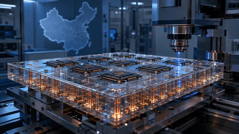
On August 7, 2026, TrendForce listed 18 publicly traded Chinese companies as part of the glass-core substrate supply chain. On July 24, Intel and Lens Technology announced a strategic collaboration on glass substrates for advanced packaging, and BOE has also begun operating a panel-level pilot line. As AI semiconductor packages grow larger, warpage and wiring density limits in organic substrates are becoming obstacles to further performance scaling. However, the number 18 does not represent the depth of mass-production-ready companies. Ahead of full-scale adoption expected from 2030 onward, Chinese firms are building out manufacturing processes, and equipment companies have begun securing orders for pilot production lines.
The 18 Companies Are Not a List of "Mass Producers"
According to TrendForce's breakdown, the supply chain is divided into three layers: raw glass and manufacturing equipment; substrate processing covering TGV formation and copper filling; and advanced packaging that mounts AI chips. The companies included in this count vary widely in their progress—from R&D, to pilot lines, to sample shipments, to equipment orders. Glass processing for displays and glass-core substrates for semiconductor packaging are also not the same product.
This distinction shows up in the details of the Intel and Lens Technology partnership. The two companies plan to accelerate development of glass substrate packaging and jointly explore key manufacturing processes for scaling toward mass production, combining Lens Technology's precision glass processing, laser processing, and large-scale production capabilities with Intel's semiconductor design and advanced packaging technology. However, the announcement only defines the scope of collaborative exploration—it does not specify product names, customers, or a mass production start date.
Still, the significance of the partnership is considerable: Lens Technology's precision glass processing capabilities have now been formally connected to AI chip packaging processes. Rather than the number of companies involved, what will determine the supply chain's actual strength is which companies pass semiconductor-grade reliability testing and secure repeat orders.
TGV Supporting 10x Wiring Density
The reason glass is needed comes down to this: as more chiplets are packed into a single package, the expansion, contraction, and warpage of organic materials make fine wiring increasingly difficult. In 2023, Intel explained that glass substrates could reduce pattern distortion by 50% compared to organic substrates and potentially increase interconnect density tenfold. Flatter, dimensionally stable materials make it easier to stack multiple layers of wiring precisely in the intended positions.
TGV (Through-Glass Via) forms conductors in fine holes drilled vertically through the glass, electrically connecting the top and bottom of the substrate. At ECTC 2026, Intel Foundry explained that it can precisely and repeatably process low-taper holes, holes of varying dimensions, and cavities for embedded components. Holes fully filled with copper reportedly passed rigorous thermal cycling tests without failure. Even if the glass itself is flat, if cracks form on the inner walls of the holes or copper fails to fill the gaps completely, the package becomes unusable. TGV is the process that translates material properties into product reliability.
Intel Foundry states that future glass substrates could integrate electrical and optical functions on a single platform. Co-Packaged Optics (CPO), which Intel presented at ECTC, is advanced packaging research aimed at higher bandwidth and lower power consumption. Specifications and timing for products combining glass substrates with CPO have not yet been disclosed. Intel plans to bring a complete glass substrate solution to market in the latter half of the 2020s.
BOE's 1,000 Panels Per Month and WG Tech's 100,000 Square Meters
At its Investor Day on July 2, 2026, BOE announced that its panel-level pilot line, designed with a monthly capacity of 1,000 panels, completed full automation line commissioning in the first half of the year. The line integrates TGV drilling, deep-hole copper filling, and build-up wiring into a single connected process, and BOE is shipping large, multilayer glass substrate samples to customers. Among the items covered under the memorandum of understanding signed with Corning in May, BOE listed glass-based package substrates and optical interconnects. However, Corning's own announcement describes the scope of collaboration more broadly as next-generation consumer devices and digital infrastructure, without going into specific products.
WG Tech presents figures even closer to mass-production equipment specs. According to the company's investor disclosures, its TGV process achieves a minimum hole diameter of 5μm, a maximum aspect ratio of 100:1, and can process glass thicknesses ranging from 0.05 to 1.1mm. The company is building a line with an annual capacity of 100,000 square meters and is shipping products for optical modules and CPO applications to customers. However, line capacity and actual utilization rate are separate figures. Sample shipments also do not equate to sustained mass production that has passed customer qualification.
What can be confirmed from both companies' disclosures is progress in bringing together equipment capable of handling hole drilling, metallization, and multilayer wiring on a single substrate. From here, customers must verify whether the same quality can be reproduced across large volumes of panels. Experience handling large-format glass in display factories serves as a starting point, but semiconductor-grade yield and durability must be built up anew.
Equipment Orders for Pilot Production Lines Move First
While substrate manufacturers await qualification, pilot lines require equipment for laser drilling, wet etching, film deposition, plating, and polishing. DR Laser disclosed that in 2024 it secured new orders for TGV equipment, including from overseas customers, covering both wafer-level and panel-level applications. As of May 2025, the company described the market as still centered on pilot production lines. There is a time lag in which orders flow to equipment companies before finished substrates generate mass-production revenue.
However, directly attributing equipment companies' overall financial results to glass substrate demand would misrepresent the actual situation. Hymson Laser's revenue for Q1 2026 was RMB 1.317 billion, up 144.36% year-on-year, with net profit turning positive at RMB 25.21 million. The company cited manufacturing sector recovery along with increased demand for lithium battery and home appliance equipment as factors behind the revenue growth. Equipment for solar and sheet metal processing also grew. The breakdown of how much TGV or CPO contributed to the revenue increase has not been disclosed.
Therefore, the industry-wide sequencing in which equipment orders arrive first must be read separately from the attribution of results to individual companies. Only once order values and delivery volumes for TGV-related equipment are disclosed can we measure how much glass-core substrates have actually boosted equipment companies' revenues.
Three Gates That Will Determine the Post-2030 Outcome
TrendForce forecasts that full-scale adoption of TGV glass substrates in advanced packaging will occur from 2030 onward. This does not necessarily contradict Intel's 2023 plan to bring products to market in the latter half of the 2020s, since it takes time to expand from initial product launches to adoption across multiple customers and use cases.
The first gate is yield: holes must be drilled while suppressing microcracks, deep holes must be filled with copper without gaps, and large-area wiring must be stacked precisely without misalignment. The second is reliability: each company must reproduce the thermal cycling test results Intel demonstrated, but at mass-production scale and under actual customer conditions. The third is customer qualification: it remains to be seen whether the samples shipped by BOE and WG Tech will pass qualification and lead to sustained orders.
The 18 Chinese companies have begun lining up across each stage of the process, from raw materials to equipment to substrate processing. The next milestone is not an increase in the number of companies involved, but rather the moment when equipment capacities like BOE's 1,000 panels per month and WG Tech's 100,000 square meters per year translate into qualified shipments and use-case-specific revenue. Once that transition is confirmed, glass-core substrates will move from being a future material for AI packaging to a component that actually shapes real supply constraints.