


When people hear that AI GPUs are hard to get, the conversation usually turns to front-end manufacturing: $400 million High-NA EUV lithography machines, 2nm production allocations, new fabs being built in Taiwan. But in September 2023, TSMC Chairman Mark Liu pointed to a different bottleneck: back-end processing.
What's in short supply isn't the AI chips themselves, but capacity in a process called CoWoS (Chip-on-Wafer-on-Substrate), which places logic dies and memory side by side on a single substrate and bonds them together. Three years later, TSMC has expanded this capacity nearly ninefold. Yet the supply-demand gap is still expected to sit at around 10% by the end of 2026, with NVIDIA alone estimated to control 60% of global demand.
September 2023: TSMC's Chairman Admits Only 80% of Demand Can Be Met
As The Register reported, Liu acknowledged at SEMICON Taiwan that TSMC could meet only about 80% of customer demand. He projected the shortage would persist for roughly 18 more months. At the time, he explained that demand for CoWoS had tripled year-over-year, and monthly production capacity would double by the end of 2024. When a foundry's chairman singles out his own back-end process as the party responsible for a supply constraint, that carries different weight than simply discussing front-end production allocations.
The numbers make the skew clear. According to an Epoch AI analysis, in 2025 the top four companies—NVIDIA, Google, AMD, and Amazon—consumed over 90% of CoWoS capacity and HBM (High Bandwidth Memory) supply by value. The same four companies accounted for only about 10% of consumption in advanced 3-5nm logic die production. AI chips barely dent front-end production allocations, but they've exhausted back-end capacity.
The reason lies in how area scales differently. A single logic die occupies a few hundred square millimeters, and a 300mm wafer can yield a substantial number of them. But CoWoS requires building a substrate that places that logic die alongside multiple HBM stacks side by side—an area that far exceeds a single reticle from a lithography machine. The back-end wafer area consumed per package dwarfs the front-end area consumed by an order of magnitude. So when trying to increase GPU shipment volumes, back-end wafer count becomes the bottleneck first.
This skew inverts a long-standing view of the semiconductor industry. For decades, the competitive axis was transistor linewidth—winners and losers shifted with each generational leap from 7nm to 5nm to 3nm. But for AI chips, securing production allocation at the most advanced node means nothing if there's no back-end capacity to ship the product. Packaging capacity availability has joined lithography generation as a criterion for choosing a foundry.
The 18-month timeline Liu cited has long since passed. TSMC has continued adding capacity nearly every year since, yet even in 2026, supply still hasn't caught up with demand. If the problem were simply insufficient production growth, throwing more capital at it would solve things. What's actually happening is that two forces are operating simultaneously: a physical constraint that money alone can't overcome, and an allocation problem where the destination for added capacity is already determined in advance.
The $100 Million Bet and 400 Engineers Nobody Wanted
The person who brought this process in-house was Shang-yi Chiang, then TSMC's co-COO. In an interview with Taiwanese media outlet bnext, Chiang testified that in 2009 he proposed to founder Morris Chang the establishment of an advanced packaging research unit, launching with 400 engineers and a $100 million capital investment. His bet was that the bottleneck in high-performance computing would shift from the transistor itself to how chips are interconnected. Some sources place the proposal year at 2006 or 2011, so it's more accurate to think of this as sometime in the late 2000s. On the scale and motivation, Chiang's own testimony remains the most concrete account.
The name CoWoS simply lists the process steps in order. First, an interposer—a relay board with wiring and TSVs (Through-Silicon Vias)—is built on a silicon wafer. Then the logic die and HBM are placed side by side and bonded onto it: this is the Chip-on-Wafer stage. Finally, that assembly is attached to a resin or ceramic package substrate: on-Substrate.
Routing the wiring between a compute die and memory through a conventional package substrate hits a limit quickly—the wires can't be made thin enough to fit the required number of connections. But an interposer built using the same lithography technology as front-end chip manufacturing can connect the two at densities far beyond what substrate wiring allows. Because the dies sit side by side rather than stacked vertically, with only the wiring pushed out to a separate silicon layer, this is called 2.5D packaging.
In 2009, the problem of high-performance compute chips being bottlenecked by memory bandwidth was still a niche concern limited to certain applications. In the world of general-purpose CPUs, advancing one process node reliably delivered better results. Chiang's proposal wasn't accepted internally at first because building an entirely new process just to shorten wiring distances didn't fit the cost logic of the time.
And for a long time, this technology found no buyers. According to Chiang's own oral history published by the Computer History Museum, the only customer to initially adopt it was Xilinx, with orders limited to just 50 wafers a month—Chiang recalls being mocked internally over it. TSMC reportedly began mass production in 2012.
From there until the generative AI boom of 2023—more than a decade—CoWoS adoption appears to have remained limited to a handful of high-performance products, staying largely unnoticed. Generative AI training and inference are processes that consume as much memory bandwidth as compute die speed, and the structure of placing HBM densely next to the compute die directly determines performance. When demand suddenly spiked, few companies could run this process at mass-production scale. The years of quietly sustained, unglamorous investment ended up creating a position that's now hard to replace.
Why Larger Interposers Warp
The reason production increases don't translate directly into supply has more to do with yield than with the number of machines available. A technical analysis from exponentialindustry cites two constraints on CoWoS expansion: material utilization drops below 70% for large interposers because square dies are cut from circular wafers, and mismatched coefficients of thermal expansion (CTE) between silicon and resin substrates cause warping in large packages measuring 120mm or more per side. Both problems share a trait: they worsen as area increases.
Here's how the warping happens. Lithography machines have a maximum area they can expose in a single pass, so interposers larger than that limit are built by stitching together multiple exposures. As the board grows larger, the difference in thermal expansion between the silicon die on top and the resin substrate below becomes more pronounced at the edges. Since the assembly process involves repeated heating and cooling cycles at each bonding step, differences in how the materials expand and contract manifest directly as warping in the board.
On a warped board, die bonding positions shift slightly, and the finer the bonding, the more this eats into tolerance margins. One would expect that increasing area would boost yield per wafer, but yield actually moves in the opposite direction. And larger interposers mean a bigger financial loss per defective unit. Since a single package already contains an expensive logic die and multiple HBM stacks, a single failure at this final stage drags down months of upstream front-end work along with it.
Die bonding itself also becomes harder as area increases. CoWoS uses a microbump method to bond the logic die and HBM onto the interposer with tiny solder bumps. If the board is warped, even a slight shift in bonding position can cause connection failures, and this tolerance margin tightens further as the area expands.
TSMC also has another 3D stacking technology for AI packaging called SoIC (System on Integrated Chips), which uses hybrid bonding to directly join copper electrodes to one another. This requires even stricter cleanliness—a single particle trapped at the bonding interface causes a defect—making it even more yield-challenging than CoWoS's microbump bonding. Packages combining CoWoS and SoIC, like AMD's MI400 series, are becoming more common, and the overall difficulty of the package continues to rise with area.
This marks a decisive difference from front-end manufacturing. A High-NA EUV machine reportedly costs about $400 million, while the average unit price calculated from ASML's full-year 2025 results for all EUV machines (combining conventional and High-NA models) comes to roughly €240 million—lower than the price range for High-NA units alone. Even with this price range, buying such equipment is a general-purpose investment where the incremental gain can be read directly in terms of linewidth and unit count.
CoWoS expansion, by contrast, depends on specialized equipment like thermocompression bonders, and industry commentary notes that procurement and certification take time. The commonly cited range is 12 to 18 months, though this isn't a figure published by equipment makers. Still, the fact that equipment models are limited in number and certification is tied to each customer's specific product is clearly different from simply adding more lithography machines.
TSMC's own capital allocation reflects this asymmetry. Its 2026 capital expenditure plan is $60 billion to $64 billion, of which the advanced packaging segment accounts for 10% to 20%. Most of the money still goes to front-end manufacturing. Yet CoWoS capacity growth is expected to post a CAGR exceeding 80% from 2022 to 2027, according to TSMC's own statement at a symposium in Taiwan, as reported by Reuters. The mismatch between capital allocation ratio and capacity growth rate reflects the fact that this process is limited more by yield and ramp-up time than by spending.
Because investment translates into capacity differently here, the growth pattern is distinctive. Lining up annual monthly capacity figures reported by TrendForce and SemiWiki produces the following:
| Date | TSMC-Only Monthly CoWoS Capacity |
|---|---|
| End of 2023 | 13,000-16,000 units |
| End of 2024 | 35,000-40,000 units |
| 2025 | ~75,000 units |
| End of 2026 (projected) | 120,000-140,000 units |
TSMC's monthly CoWoS capacity has expanded from 13,000-16,000 units at the end of 2023, to 35,000-40,000 units at the end of 2024, to roughly 75,000 units in 2025, with a projected 120,000-140,000 units by the end of 2026—roughly a ninefold increase over three years (all figures represent TSMC's own production lines, excluding OSAT partner capacity). Estimates for 2026 vary by source. Even so, a roughly ninefold expansion over three years is an unusually rapid pace of capacity buildout for an equipment-intensive industry. Given how many years it typically takes a new front-end fab to go from groundbreaking to mass production, it's hard to characterize a process that increased capacity tenfold over the same timeframe as "slow to expand." And yet this process remains sold out.
Why Estimates for End-2026 Capacity Range from 90,000 to 140,000 Units
Publicly available estimates for TSMC's own CoWoS monthly capacity at the end of 2026 haven't converged on a single figure. On June 15, 2026, TrendForce reported figures of 120,000 to 140,000 units, citing institutional investor information relayed by Economic Daily News. Meanwhile, a compiled table published by SemiWiki puts the same 2026 figure at 90,000 to 110,000 units. Whether comparing upper bounds or lower bounds, the gap runs to roughly 30%.
The most straightforward explanation for this discrepancy is timing. The SemiWiki table doesn't specify when its source data was published, and the June 2026 TrendForce report likely reflects more recent information. Even if we favor the more recent figure, discarding the range entirely changes how tight the supply situation feels. Under the same headline of "capacity expanding," a world of 90,000 units a month and a world of 140,000 units a month mean very different wait times for customers seeking allocation.
When reading capacity figures, it's worth first confirming whether they represent TSMC alone or the industry total including OSAT partners, and whether they're monthly or annual figures. Even discussing the same year, 2026, TSMC's own monthly figure of 120,000 to 140,000 units is a different thing from an industry-wide figure approaching 200,000 units that includes OSAT capacity. The gap with SemiWiki's 90,000 to 110,000 figure may also stem from differences in scope and timing. The fact that the numbers haven't settled into a single consensus is itself evidence that this market's outlook remains unsettled.
Demand-side figures also show a wide range. Silicon Analysts estimates global CoWoS demand for 2026 at roughly 1 million units, with lead times reaching 52 to 78 weeks, keeping the market fully booked. A more recent analysis from exponentialindustry, dated August 2026, estimates global demand at 1.3 million to 1.4 million units in 2026, doubling to 2.5 million to 2.7 million units in 2027—a notably higher figure than Silicon Analysts' estimate. Regardless of which figure one takes, the analytical direction is consistent: advanced packaging allocation itself has become a constraint on AI hardware.
Behind demand growth lies a factor that can't be explained by GPU shipment volume alone. As training cluster scale increases, HBM content per unit rises, meaning interposer area consumption grows even at the same unit volume. Meanwhile, custom ASICs (Application-Specific Integrated Circuits) from Google and Amazon have entered mass production, increasing the variety of designs using CoWoS. Demand for units is growing as the product of chip count, area, and design variety.
TrendForce reported that the supply gap will narrow from roughly 20% currently to about 10% by the end of 2026. Capacity increases ninefold over three years, and the gap is cut in half. It doesn't reach zero.
Even as the gap ratio narrows, procurement doesn't get easier, because long lead times change how allocation gets decided. If securing capacity a year to a year and a half in advance is necessary to receive actual product, orders must be placed before demand is even confirmed—while it's still a forecast. Companies that can lock in capacity early through prepayment or long-term contracts gain an advantage, while those whose demand grows later must search for whatever's left.
Under this structure, even if the supply gap shrinks to 10%, who ends up short doesn't get decided evenly. Those holding allocation ship products as planned; only those without it wait. A technical wall sets the upper limit on capacity, and lead time determines how that limit gets distributed. From here, what moves things forward isn't a law of physics. It's who signed a contract, and when.
AMD, Broadcom, and Google Fighting Over the Remaining 400,000 Units
That distribution is now heavily tilted toward NVIDIA. According to Morgan Stanley estimates that multiple outlets have reported, NVIDIA is projected to secure 595,000 units of CoWoS capacity in 2026, combining TSMC's own production lines with output from Amkor and ASE-affiliated OSATs. This 60% figure rests on a single analyst report and hasn't been confirmed by TSMC itself.
Still, cross-referencing this estimate against 2026 demand projections turns other companies' situations into concrete numbers. If global demand is roughly 1 million units and NVIDIA secures 595,000, that leaves roughly 405,000 units for everyone else. AMD, Broadcom, Google, Amazon, and other companies launching custom ASICs must divide this remainder among themselves. This subtraction shifts depending on which demand estimate is used—using exponentialindustry's higher figure of 1.3 to 1.4 million units, the remainder becomes 700,000 to 800,000 units. Either way, the structural picture stays the same: the allocation shared by everyone besides NVIDIA is far smaller than total demand.
This remainder of roughly 400,000 units effectively sets the ceiling on the AI semiconductor competitive landscape. Training GPU and inference ASIC designs grow larger every year, and interposer area consumed per package increases with each generation. The same number of units yields fewer packages once companies switch to next-generation products. In other words, every company below NVIDIA in the ranking must simultaneously negotiate for more allocation and work to design smaller packages.
Allocation slots are already filling up years in advance. DigiTimes reported observations that NVIDIA has secured more than half of TSMC's total 2026 CoWoS capacity, with a similar ratio expected to continue into 2027. If ownership shares are largely fixed before new production lines even come online, the effective availability for other companies won't grow at the same pace as overall capacity. Estimates circulating suggest Broadcom's 2026 allocation is roughly 185,000 units, up 93% year-over-year, while AMD's is roughly 90,000 units, up 64%.
TSMC itself isn't standing still, either. TrendForce reported that TSMC is expanding its practice of outsourcing certain pre-CoWoS process steps to Amkor and ASE subsidiary SPIL. If the additional 50,000 to 60,000 units of monthly capacity from OSAT partners materializes, industry-wide monthly capacity would approach 200,000 units. Since ramping up in-house lines is constrained by yield learning curves, spinning off process steps to OSATs that already have equipment and personnel in place makes sense as a way to buy time.
The absence of a mature alternative supplier is another reason the oligopoly hasn't loosened. Samsung offers I-Cube largely for its own customers, and Intel has EMIB and Foveros. But no supplier currently matches TSMC at mass-production scale. Tom's Hardware has even reported that CoWoS tightness is creating an opportunity for Intel's back-end technology. If the primary allocation slots were actually open, alternative technologies wouldn't be discussed this much.
The yield wall and the allocation wall differ in character. The former is a physical problem that worsens as area expands—one where capital investment has a speed limit on how fast it can overcome the constraint. The latter is a contractual problem about who secured slots first—physically solvable, but requiring a restructuring of the supply chain to move. The forecast of a 10% gap remaining by the end of 2026 makes more sense read as the combined result of these two forces operating at once.
Glass Substrates, Grinding Equipment, and Japan's Rising Role in the CoPoS Transition
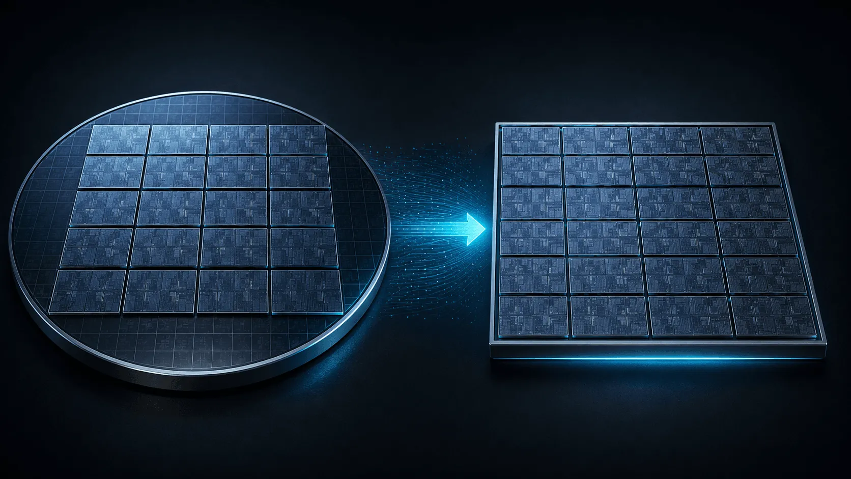
Efforts to push back the area limit are already underway within CoWoS itself, without waiting for next-generation technology. At its April 2026 technical symposium, TSMC revealed it is already mass-producing CoWoS with 5.5x reticle size. The company plans to introduce a 14x reticle CoWoS package fitting roughly 10 compute dies and 20 HBM stacks into a single package by 2028, followed by an even larger version exceeding 14x by 2029 (per TSMC's official statements).
Beyond that lies another answer: CoPoS (Chip-on-Panel-on-Substrate). According to TrendForce, TSMC launched a CoPoS R&D line at subsidiary VisEra in 2025, working toward material and equipment certification with a target completion of June 2026. Trial production is expected to begin in mid-2027, with mass production ramping up in Chiayi and Arizona between 2028 and 2029. The first adopting customer is expected to be NVIDIA's Feynman platform.
The reasoning behind moving from round wafers to square panels comes down to how area gets used. Because CoWoS builds interposers on a circular 300mm wafer, the larger the rectangular package being cut, the more unusable space accumulates near the circle's edge. As packages grow larger, this inefficiency becomes an increasingly unavoidable loss. Square panels can tile rectangles without gaps, increasing the number of packages obtainable from the same area. This creates a two-stage approach: CoWoS's own reticle expansion first pushes back the area limit, and CoPoS steps in as the backstop for generations where that still isn't enough.
Japanese materials and equipment makers are increasingly named in this transition. Ibiden is reportedly planning to jointly develop mass production of glass-core substrates for CoPoS with TSMC and Innolux. The presence of Innolux, which has handled large-format glass in panel display manufacturing, speaks to the nature of this transition—technology for precisely handling large, square surfaces has developed further in LCD production lines than in semiconductor back-end processing. However, TrendForce reports that commercial mass production of glass-core substrates will come even later than CoPoS's trial and initial mass production phases, meaning it won't immediately become the primary material when CoPoS ramps up between 2028 and 2029.
The reason for using glass as a substrate core directly answers the warping problem seen earlier. Glass offers better flatness and dimensional stability than resin, resisting dimensional shifts through repeated heating and cooling cycles. As panels grow larger, this difference translates directly into yield through reduced edge-position shifting. TSMC is pushing back against the warping and CTE-mismatch constraints seen in CoWoS from the materials side as well. This is why Japanese companies with strong package substrate technology, including Shinko Electric Industries, are increasingly named in this space.
Lining up the timeline also makes clear that this transition won't ease the current squeeze. If CoPoS trial production begins in mid-2027 and mass production comes in 2028-2029, the 2026 allocation battle will still be settled within CoWoS itself. Near-term relief will come from CoWoS's own reticle expansion and outsourcing, with CoPoS playing the role of the next backstop once area limits become even more acute.
On the equipment side, Disco's position remains unshaken. The company reportedly holds a 70% to 80% global share in both dicing saws and grinders, giving it a strong position in cutting interposers and grinding HBM to thin profiles. Reports indicate that Disco equipment made up much of the grinding equipment adopted even on TSMC's CoPoS trial line. If ASML is the star of front-end manufacturing, Japanese equipment makers hold significant presence in the cutting and grinding processes that determine back-end yield.
The Constraint Doesn't Disappear—It Just Moves
The capacity shortage Mark Liu named in 2023 remains unresolved even after a ninefold expansion. Two overlapping reasons explain why. One is the yield wall: interposer warping, mismatched thermal expansion between materials, and low material utilization from cutting squares out of round wafers. This constraint doesn't respond to simply adding more equipment the way EUV lithography does. The other is the order of allocation—TSMC's total capacity is more than half claimed by NVIDIA in advance—and this is determined not by physics but by contract.
Looking at either factor alone fails to explain the numbers. If the yield wall were the sole cause, it wouldn't square with TSMC's track record of a ninefold expansion in three years. If allocation skew were the sole cause, then given TSMC's incentive to expand capacity and sell it all, supply should catch up as prices rise. Only by reading both factors as operating simultaneously does the end-2026 outlook—a ninefold expansion that still leaves a 10% gap—make sense.
On paper, some signs point toward easing. TrendForce reported that TSMC plans to expand CoWoS capacity by more than 60% further by 2027. Including the additional 50,000 to 60,000 monthly units added through OSAT outsourcing, industry-wide monthly capacity could approach 200,000 units within 2026. Tracking the supply-demand gap ratio alone, 2027 should be easier than 2026.
But CoPoS represents a transition that requires recertifying both materials and equipment from scratch. Will glass-core substrates achieve good yields at large area without cracking or warping? Will per-panel yield exceed per-wafer yield? Will material and equipment certification, targeted for June 2026, finish on schedule? If all three conditions are met, CoPoS will push the area limit that CoWoS's own reticle expansion (14x by 2028, larger still by 2029) has already begun opening up—allowing compute and memory bandwidth to grow together even further. If they aren't met, the bottleneck simply moves from wafer to panel.