

Peer through a microscope at a superconducting quantum computer chip, and you'll notice one component occupying a disproportionately large area: arrays of Josephson junctions. To realize fluxonium—a type of qubit—or the "superinductance" essential for superconducting detectors, structures with 80 to several hundred Josephson junctions connected in series consume precious space on the chip.
A material that could fundamentally solve this area problem has been drawing attention since the mid-2010s: the single atomic layer of niobium diselenide (). This three-atom-thick structure (roughly 1 nm thick), in which a densely packed layer of niobium atoms is sandwiched from above and below by monolayers of selenium atoms, exhibits an extraordinarily large kinetic inductance—that is, the inductance stored per unit area. In 2016, Xi et al. observed a peculiar state called "Ising superconductivity" in monolayer (Nature Physics, 2016), demonstrating that this material is also rich in fundamental physics.
However, this material had a fatal weakness: it degrades through oxidation the instant it contacts air.
A Material That Breaks the Moment It's Synthesized: The Limits of "Post-Hoc Protection"
Conventional methods for handling monolayer fell broadly into two categories. One is mechanical exfoliation, in which thin flakes are peeled from a bulk crystal. Samples obtained this way are limited to a few micrometers square, and it is difficult to reproducibly obtain uniform monolayers. The other is chemical vapor deposition (CVD) synthesis on a substrate, followed by capping with a protective layer of graphene or hexagonal boron nitride (hBN) after synthesis.
The latter approach has a fundamental timing problem. begins to oxidize the instant synthesis is complete. In the seconds to minutes it takes to apply the protective layer, the surface degrades and superconducting properties are compromised. Zheng, a member of the research team, stated: "Normally, the moment you synthesize the material and remove it from the inert environment, oxidation and degradation begin, and it eventually falls apart."
This degradation goes beyond mere surface contamination. X-ray photoelectron spectroscopy (XPS) analysis has confirmed that in oxidized , the niobium valence shifts from 4+ to 5+, and the selenium signal disappears entirely. The product is niobium pentoxide (), and superconductivity is completely lost.
The Principle of Encapsulation Epitaxy: Growing Within a Gap
The "encapsulation epitaxy" technique devised by the MIT research team is based on a conceptual shift: building the protection step into the growth process itself, rather than applying it after growth.
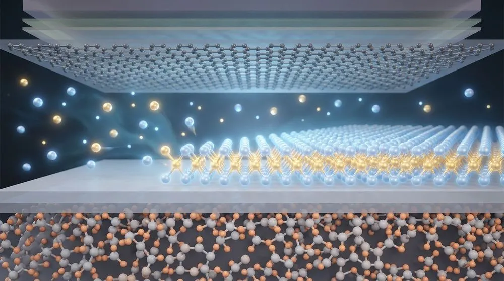
The procedure is as follows. First, a monolayer of graphene is pre-transferred onto a silicon dioxide () substrate. The van der Waals forces between graphene and are weak, and a tiny gap of less than 1 nm naturally forms between them. Next, chemical precursors of niobium and selenium are supplied onto this structure. The precursors infiltrate the gap through the edges and defects of the graphene, adsorbing onto the surface to form crystal nuclei. While the substrate captures the precursors and promotes crystallization, the overlying graphene permits in-plane diffusion of the precursors, guiding the formation of a uniform monolayer.
Growth proceeds only within the gap. The research team confirmed via low-temperature dry pick-up experiments that no forms on the upper surface of the graphene. After peeling away the hBN protective layer, remained on the substrate, with nothing attached to the hBN side.
By the time growth is complete, the is already encapsulated by graphene. It does not oxidize even when removed into ambient air. Films obtained by this method are continuous monolayers exceeding one inch (about 2.5 cm) in size, with atomically smooth surfaces.
Zheng, the paper's first author, remarked: "It took a long time to understand how growth occurs beneath the graphene. Through collaboration and discussion, we clarified the growth mechanism at the interface, resolved many issues, and were able to simplify the fabrication process."
Integration into Circuits: Verifying Edge Contacts and Kinetic Inductance
Simply producing a large-area thin film is not enough for application to quantum circuits. The research team developed two additional processes.
First, an oxidation-free transfer method. Building on a technique established in prior work (Nature, 2025), the graphene/ structure is peeled from the growth substrate and moved onto the target circuit substrate.
Second, formation of electrical connections. It is necessary to reliably connect the roughly 1-nm-thick film to electrodes several hundred nanometers thick. The research team adopted an "edge contact" structure, in which the film's side edges are carefully etched in vacuum to expose smooth end faces, which are then brought into contact with superconducting electrodes.
Following this process, measurements were performed integrating into superconducting microwave circuits. The results showed that the material retained superconductivity even after cleanroom processing, with a measured kinetic inductance of ≈ 0.7 nH/□. In a separate experiment previously reported by the team (Nature Communications, 2026), few-layer encapsulated with hBN reached up to 1.2 nH/□—one of the highest sheet kinetic inductances reported at the monolayer limit.
Comparison with Existing Superinductance Methods
Here we position monolayer relative to existing methods for realizing superinductance.
| Method | Material | Sheet Kinetic Inductance | Area Characteristics | Air Stability |
|---|---|---|---|---|
| Josephson junction array | Al/AlO/Al junction | ~0.5–1 nH per junction | 80–160 junctions needed for 100–300 nH | Stable |
| Amorphous thin film (TiN, NbTiN, gr-Al) | Amorphous superconductor | 0.1–several nH/□ (depends on film thickness) | Increases as film is made thinner | Varies by material |
| Monolayer (this study) | Crystalline van der Waals superconductor | 0.7–1.2 nH/□ | Achieved with a single atomic layer (~1 nm) | Air-stable via graphene encapsulation |
Josephson junction arrays, the standard method for achieving superinductances of 100–300 nH, have been widely used since Masluk et al. (PRL, 2012) first demonstrated the approach, but the required area grows in proportion to the number of junctions. Because monolayer provides this function at atomic-scale thickness, it may be possible to achieve the same inductance in a far smaller area.
In addition, the self-Kerr nonlinearity of monolayer is small, at = −0.008 to −14.7 Hz/photon, meaning large linear inductance can be exploited without significant nonlinear effects—making it well suited for shunt inductors in fluxonium qubits and for microwave photon detectors.
The Generality of Encapsulation Epitaxy: Beyond
The technique presented in this study is not unique to . The research team demonstrated that this growth strategy, using graphene or hBN as the encapsulating layer, can be extended to a diverse family of monolayer quantum materials. The combination of encapsulating layer and substrate is also not limited to graphene/; it functions in multiple systems including graphene/ and hBN/. However, monolayer growth has not been confirmed on or substrates, indicating there are constraints on substrate selection.
Another advantage brought by encapsulation epitaxy is interface cleanliness, resulting from growth and encapsulation occurring simultaneously. In conventional post-hoc transfer methods, polymer residues or adsorbed molecules tend to become trapped between the protective layer and the superconductor. Because encapsulation epitaxy forms the interface without any contact with air, an atomically clean van der Waals interface is obtained.
Remaining Questions
The superconducting transition temperature, ≈ 1 K, is markedly lower than the 7.2 K of bulk . While this reduction in transition temperature at the monolayer limit is a known phenomenon in the context of Ising superconductivity, and although there remains sufficient margin relative to the operating temperature of quantum circuits (typically 10–20 mK), extending this approach to material systems with higher remains an important direction.
Also, detailed evaluation of quality factor (Q) and microwave losses after circuit integration remains a task for future verification. A prior report from IOP Science achieved in superconducting microwave resonators using , but systematic loss measurements on monolayer films grown via encapsulation epitaxy have not yet been sufficiently established.
Furthermore, it remains uncertain how far this technique can be developed into a mass-production process worthy of the label "wafer-scale." A continuous film exceeding one inch represents major progress at the laboratory level, but scaling to the 300 mm wafers used in the semiconductor industry leaves engineering challenges outstanding, such as large-area graphene transfer technology and uniformity of precursor supply.
Encapsulation epitaxy has brought a group of 2D superconductors—whose research had been confined to small-scale flakes simply because they could not be handled in air—onto the table of circuit design. How far a single atomic layer of material can expand the design freedom of quantum hardware is a question whose next stage depends on device-level verification.