

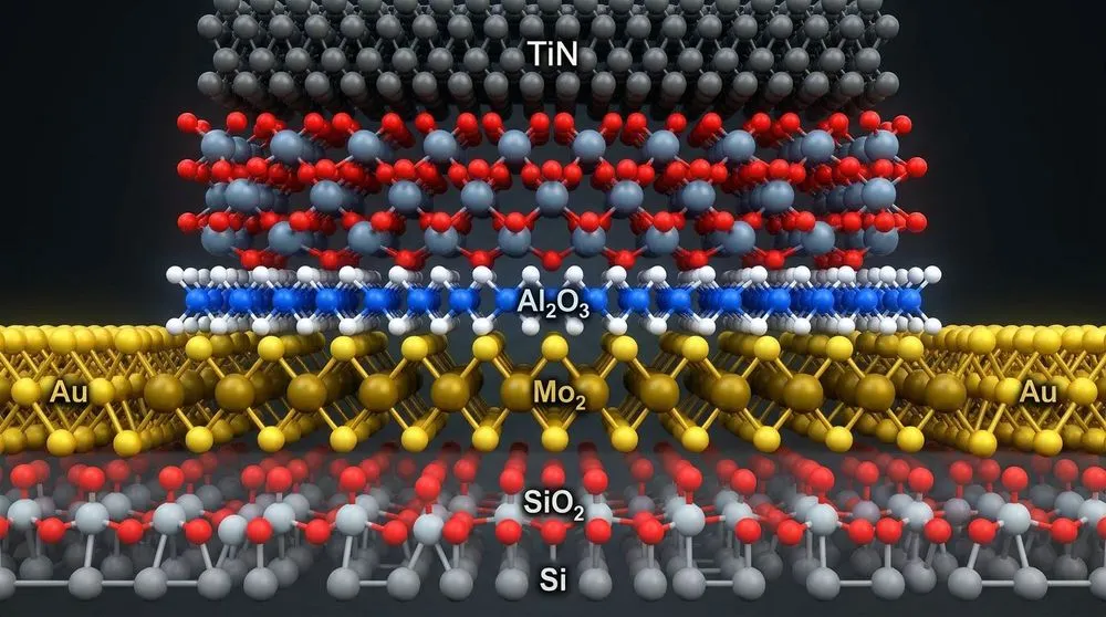
In 2011, when a Stanford University team first operated a field-effect transistor made from monolayer MoS₂ (molybdenum disulfide), researchers' expectations were clear. This semiconductor, only a single atomic layer thick, is structurally unconstrained by the sharp mobility loss that silicon channels suffer once thickness drops below 3nm. As gate lengths of 12nm and below come into view for future logic semiconductors, it has come to be regarded as the leading candidate channel material to replace silicon.
However, this very "thinness" created a different wall. Shrinking transistors requires thinning the insulating film (gate dielectric) sandwiched between the gate electrode and the channel, in order to strengthen electrostatic control. This process, optimized over decades in silicon technology, is fundamentally difficult with 2D materials. Because the surface of MoS₂ lacks dangling bonds, there are almost no reactive nucleation sites for the precursor molecules used in atomic layer deposition (ALD) to adsorb onto, so the dielectric grows only in isolated islands. The result is pinholes (tiny gaps), which increase leakage current, while interfacial defects scatter carriers and degrade mobility.
This problem remained unresolved in 2D transistor research for more than a decade.
A structure that cannot have it both ways
One metric that governs 2D transistor performance is transconductance (). It indicates how much the channel current responds to a small change in gate voltage, and it directly determines voltage gain and switching speed. Raising requires lowering EOT (equivalent oxide thickness, i.e., the effective thinness of the dielectric), shortening the channel length, and maintaining carrier mobility—all at once.
The problem is that these three requirements tend to conflict with one another. Pushing EOT below 1nm intensifies scattering from dielectric polarization fluctuations and interfacial defects (dielectric-induced scattering), which lowers mobility. Lower mobility, in turn, caps . A theoretical simulation published in npj 2D Materials and Applications in 2026 reported that bonding amorphous Al₂O₃ to monolayer MoS₂ can reduce mobility by as much as 70%.
Past research has attacked this trade-off with various seed layers (PTCDA molecules, thin Si films, thin Ge films, etc.), van der Waals stacking, and plasma-based surface activation. Some approaches pushed EOT down to 0.67nm, but these were experiments using exfoliated flakes (micro-crystals mechanically peeled from bulk material); no report had simultaneously achieved an EOT near 1nm and high using wafer-scale CVD-grown films.
Changing the boundary, not the material
A joint research team led by Professor Chang Wen-Hao of NYCU's Department of Electrophysics and Tsung-En Lee of TSMC Corporate Research shifted the axis of the approach. Rather than searching for a new semiconductor material or developing a new dielectric material, they made the "boundary" between the two the object of design itself.
The method proceeds as follows. First, monolayer MoS₂ grown by CVD on a sapphire substrate is transferred onto a target substrate. Next, a 0.3nm-thick aluminum film is epitaxially grown on the MoS₂ by electron-beam evaporation under ultra-high vacuum. Because this aluminum grows in an arrangement that matches the surface structure of MoS₂, it forms a uniform, continuous film. This is followed by in-situ, low-pressure oxidation, converting the aluminum into an Al₂O₃ (aluminum oxide) layer roughly 0.42nm thick. Finally, 2.85nm of HfO₂ (hafnium oxide) is deposited on top of this Al₂O₃ by ALD, completing the gate dielectric stack.
The 0.42nm Al₂O₃ layer serves two roles. First, it provides a smooth, continuous growth platform for HfO₂, which cannot nucleate uniformly on the dangling-bond-free surface of MoS₂. Second, by inserting an atomic-scale buffer layer between the MoS₂ channel and the HfO₂ dielectric, it suppresses the scattering that dielectric polarization fluctuations and interface states would otherwise inflict on electrons in the channel.
Professor Chang stated in a press release: "For years, improving 2D transistors has focused on searching for better semiconductor materials. Our work shows that the atomic interface between materials matters just as much."
Numbers showing all three goals achieved at once
The top-gate transistor (channel length about 100nm) fabricated using this interface design shows a clear advance over previously reported CVD-grown monolayer MoS₂ devices.
| Metric | Previous best (CVD monolayer MoS₂, top-gate) | This study |
|---|---|---|
| EOT | ~2nm (7nm HfO₂, Ref. 17) | 1.06nm (0.42nm Al₂O₃ + 2.85nm HfO₂) |
| Peak transconductance | 0.31 mS/μm (channel length 750nm) | 0.45 mS/μm (channel length ~100nm) |
| Subthreshold swing SS | 71.4 mV/dec (Ref. 17) | ~75 mV/dec |
| Channel material | CVD-grown monolayer MoS₂ | CVD-grown monolayer MoS₂ |
While roughly halving EOT (from 2nm to 1.06nm), improved by about 45%, from 0.31 to 0.45 mS/μm. The channel length was also shortened from 750nm to about 100nm, and the fact that this value was achieved while suppressing short-channel effects is noteworthy. In addition, gate leakage current remained low, and hysteresis (the shift in characteristics depending on the sweep direction of gate voltage) was kept to a minimum.
Professor Lee stated: "When the building blocks of a transistor are only a few atomic layers thick, the interface is no longer just a boundary between materials—it becomes an active part of the device."
Reach toward wafer-scale manufacturing
Another significant aspect of this research lies in the starting point of the material. Many previous high-performance 2D transistors used tiny flakes peeled from layered crystals with adhesive tape (exfoliated flakes). While exfoliated flakes offer high crystal quality, their size is limited to tens of micrometers, making them unsuitable for circuit integration. This study uses monolayer MoS₂ grown at wafer scale by CVD, giving it strong compatibility with future mass-production processes.
Indeed, the industrialization of 2D materials is advancing rapidly. In June 2026, a joint team from imec, ASML, and TSMC presented results at the VLSI Symposium on fabricating MoS₂ nFETs and WSe₂ pFETs on 300mm wafers at a 50nm contact poly pitch. TSMC Senior Vice President and CTO Min Cao has stated that "the focus is on accelerating the move from lab to fab," and the interface engineering approach in this study fits within that same trend.
The IRDS (International Roadmap for Devices and Systems) envisions the introduction of 2D semiconductors as channel materials at the 0.7nm node in 2034. The device structure at that point is expected to be gate-all-around (GAA), with a target gate length of 12nm and a contact gate pitch of 38nm. The EOT of 1.06nm achieved in this study is close to the level of dielectric scaling this roadmap demands.
Questions that remain
While the direction this result points toward is clear, many points must still be verified before practical application. First is uniformity across the full wafer. This study is a demonstration on individual devices, and variability across arrays of hundreds or more transistors has not been reported. Next is thermal stability. The Supplementary Data confirms characteristic improvements after a 400°C forming-gas anneal, but mass-production processes may involve even higher-temperature steps, and it remains unclear how well the structural stability of the epitaxial Al₂O₃ layer would hold up under such conditions.
Applicability to p-type channel materials (such as WSe₂ or WS₂) has also not been verified. The surface electronic structure differs between n-type MoS₂ and p-type WSe₂, and there is no guarantee that the aluminum epitaxial growth conditions used here can be directly transferred. In addition, the of 0.45 mS/μm achieved in this study is still more than an order of magnitude lower than that of state-of-the-art silicon FinFETs (several mS/μm); for 2D materials to replace silicon, further improvements in mobility and contact resistance will be required.
The idea of "designing" an interface is not itself new in semiconductor engineering. In silicon technology, quality control of the Si/SiO₂ interface has long determined MOSFET performance. The question now is how device behavior changes when that interface, in 2D materials, is deliberately constructed as a 0.42nm-thick film. This study presents, as peer-reviewed data, a first step toward answering that question.