

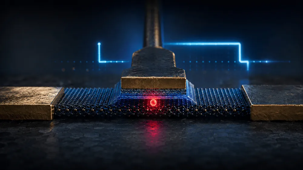
A research team at Fudan University has developed a two-dimensional memory device capable of reading the movement of a single electron as a 0.5V voltage difference. The threshold voltage shift observed at 27°C demonstrates non-volatility, and by using atomically thin materials combined with coplanar electrodes, the team suppressed the parasitic capacitance that would otherwise weaken such a minute charge signal. The results were published in Science on July 16, 2026. Since room-temperature storage of a single electron was already achieved 29 years ago, the value of this work does not lie in being the "first single-electron" demonstration. Rather, it lies in expanding a signal that previously measured only about 55mV and lasted a mere 5 seconds into a clear 0.5V signal that transistors can readily distinguish, while also achieving non-volatile operation.
How Does This Differ from the Room-Temperature Demonstration 29 Years Ago?
Room-temperature operation of single-electron memory was already demonstrated in Science back in 1997. L. Guo and colleagues combined a silicon channel roughly 10nm wide with a polysilicon floating gate approximately 7nm square and 2nm thick. As the charging voltage was increased continuously, the threshold voltage shifted in discrete steps of about 55mV, each corresponding to a single electron.
However, this device lacked an intentional tunnel oxide layer, and the charge on the floating gate leaked away in about 5 seconds after the control gate was grounded. While the 1997 paper demonstrated that a single electron could be counted at room temperature, it fell short of achieving long-term retention as a true memory.
| Comparison Point | 1997 Silicon Device | 2026 Two-Dimensional Device |
|---|---|---|
| Operating Temperature | Room temperature | 27°C |
| Threshold Change per Electron | ~55mV | 0.5V |
| Retention | ~5 seconds | Non-volatile threshold shift |
| Central Challenge | Room-temperature detection of a single electron | Achieving a large, readable signal and non-volatile operation |
0.5V is approximately 9 times larger than 55mV, and this difference carries real significance for circuit design. For a memory circuit to distinguish between "0" and "1," it needs enough read margin to separate states despite device-to-device variation and electrical noise. By boosting the change produced by a single electron from tens of millivolts to 0.5V, a single electron moves closer to being something that can be clearly read as a transistor state, rather than merely something detectable in a physics experiment.
The Coplanar Drain-Channel-Source Structure That Produced 0.5V
The threshold voltage shift achievable by moving a single electron depends on the charge divided by the device's capacitance. The 1997 paper expressed this relationship roughly as "ΔVth ≈ e/(Cdg + Cfrg)." Here, Cdg is the capacitance between the control gate and the floating gate, while Cfrg is the fringing capacitance that wraps around from the channel side. The larger this fringing capacitance, the more the effect of a single electron gets diluted, causing the voltage step to sink into noise.
Threshold voltage refers to the gate voltage at which a transistor begins to conduct current. When an electron is added to the floating gate, it shifts the voltage required to open the channel. Memory devices read this shift and convert the presence or absence of the electron into a bit. Therefore, the 0.5V figure represents not the amount of stored charge itself, but rather how large a difference a single electron can convey to the readout circuit.
In the older device, the estimated fringing capacitance reached roughly 100 times the inter-gate capacitance. Even at the time, the authors pointed out that reducing the fringing capacitance could yield a change larger than 55mV. However, shrinking the device tends to relatively strengthen the influence of the channel sidewalls, meaning that simple miniaturization can actually make a single electron harder to detect. This paradox persisted for a long time.
Fudan University's device aligns the drain, channel, and source within the same plane, self-aligning the gate, the charge-storage layer, and the channel. By using an atomically thin two-dimensional channel and edge contacts, it minimizes the electric field wrapping around from three-dimensional channel sidewalls. This coplanar structure suppresses the parasitic fringing capacitance that arises between the gate and channel, enabling a single electron to produce a 0.5V non-volatile shift.
Beyond the atomically thin materials, the geometric structure that determines capacitance plays a key role. Since the charge of a single electron cannot be changed, the team instead reduced the capacitance upon which that charge acts, extracting a larger voltage difference from the same single electron. In effect, they restructured the device layout to counteract the parasitic effects that miniaturization tends to amplify.
A "Quantum Memory" That Still Stores Classical Bits
The new device also exhibited discrete behavior in the voltage used to write charge. Shushen Li of the Institute of Semiconductors, Chinese Academy of Sciences, discussing this research in an editorial in the Journal of Semiconductors, explained that the minimum program voltage needed to advance to an adjacent state was quantized, and that within the measured range, the threshold change showed almost no dependence on pulse duration. In other words, even as the voltage is increased incrementally, the memory state does not shift smoothly and continuously—it switches at discrete steps corresponding to the electron count.
The research team further proposed a theory they call the "density-of-states scissors." By designing the electron density of states in the storage layer, they predicted that a certain quantum state would disappear partway through, and they observed a corresponding phenomenon using a self-aligned dual-Dirac structure. This goes beyond the operation of counting electrons one by one, opening up the possibility of selecting the very storage states available through the material's electronic structure.
At the same time, the information this device stores is a classical bit represented by "whether an electron is present or absent." This is not a demonstration of quantum computer memory capable of holding arbitrary quantum superpositions or preserving quantum entanglement. The word "quantum" here refers specifically to the exploitation of the discrete energy states and programming behavior of a single electron.
Li estimated the programming energy of the new device at approximately 5aJ (attojoules) per bit. This is a device-level estimate, not the power consumption of a memory array that includes wiring, selection transistors, and readout circuitry. Nevertheless, having extended a single-electron signal up to 0.5V, this figure does suggest the possibility of simultaneously pursuing extremely small write charges and adequate read margins.
Also, the 5aJ figure is an estimate of the energy delivered to the device for a single write operation; it does not include standby leakage power or the amplification cost during readout. To evaluate this as a product, one would need to add the power consumed by the peripheral circuitry that drives the cells. The device-level figure cannot be directly translated into power-efficiency improvements for smartphones or data centers.
The Distance Between 1 Electron/Bit and High-Capacity Chips
"1 electron per bit" is a claim that the lower limit on the number of electrons used for charge storage has been reached. It does not mean that per-area capacity of a chip has reached its theoretical limit. Factors such as cell footprint, interference with neighboring cells, selection circuitry, and wiring margins all remain, so reducing the number of electrons carrying a single bit does not automatically maximize the number of bits that can fit in a given area.
The same research group at Fudan University has a track record of integrating two-dimensional flash memory. In a 2024 Nature Electronics paper, they fabricated 1,024 devices using a different MoS2 channel structure than the one used here, reporting a yield exceeding 98%. The channel was scaled down below 10nm, and the devices also demonstrated storage of up to 4 bits and endurance exceeding 100,000 cycles.
In a 2025 Nature paper, a different graphene-channel device achieved 400ps write speeds and endurance exceeding 5.5 million cycles. That 400ps device, with a channel length of 0.2µm, operated at 5V. The same group has continued to advance miniaturization and integration while also improving speed and endurance in separate prototype efforts. However, these figures belong to different device architectures and cannot be directly carried over to the single-electron memory discussed here.
The next step is to align the 0.5V steps across a large number of cells. Since the outcome depends on a single electron, variation between cells must be tightly controlled. Once retention time and rewrite endurance can be measured across large-scale arrays, and once the read margin afforded by a single electron can be maintained even when peripheral circuitry is included, the physical limit on charge count will finally translate into gains in chip capacity and power efficiency.