


On August 24 local time, Fujitsu detailed the internal architecture of its data center Arm CPU, "FUJITSU-MONAKA," at Hot Chips 2026. Evaluation samples with 144 cores have already begun shipping, with mass production planned for 2027. What's new isn't the core count on a 2nm process—it's the decision to move the entire last-level cache (LLC) and power circuitry to a 5nm base die, then stack 2nm cores on top. It's a design that separates circuits that drive performance from circuits where shrinking process nodes offers little cost benefit.
2nm Accounts for Less Than 30% of Total Silicon Area
The MONAKA package contains four core dies, each holding 36 cores, with four SRAM dies stacked directly beneath them. An I/O die sits at the center. The core dies are manufactured on TSMC's N2P process, while the SRAM and I/O dies use N5—meaning N2P accounts for less than 30% of the total silicon area.
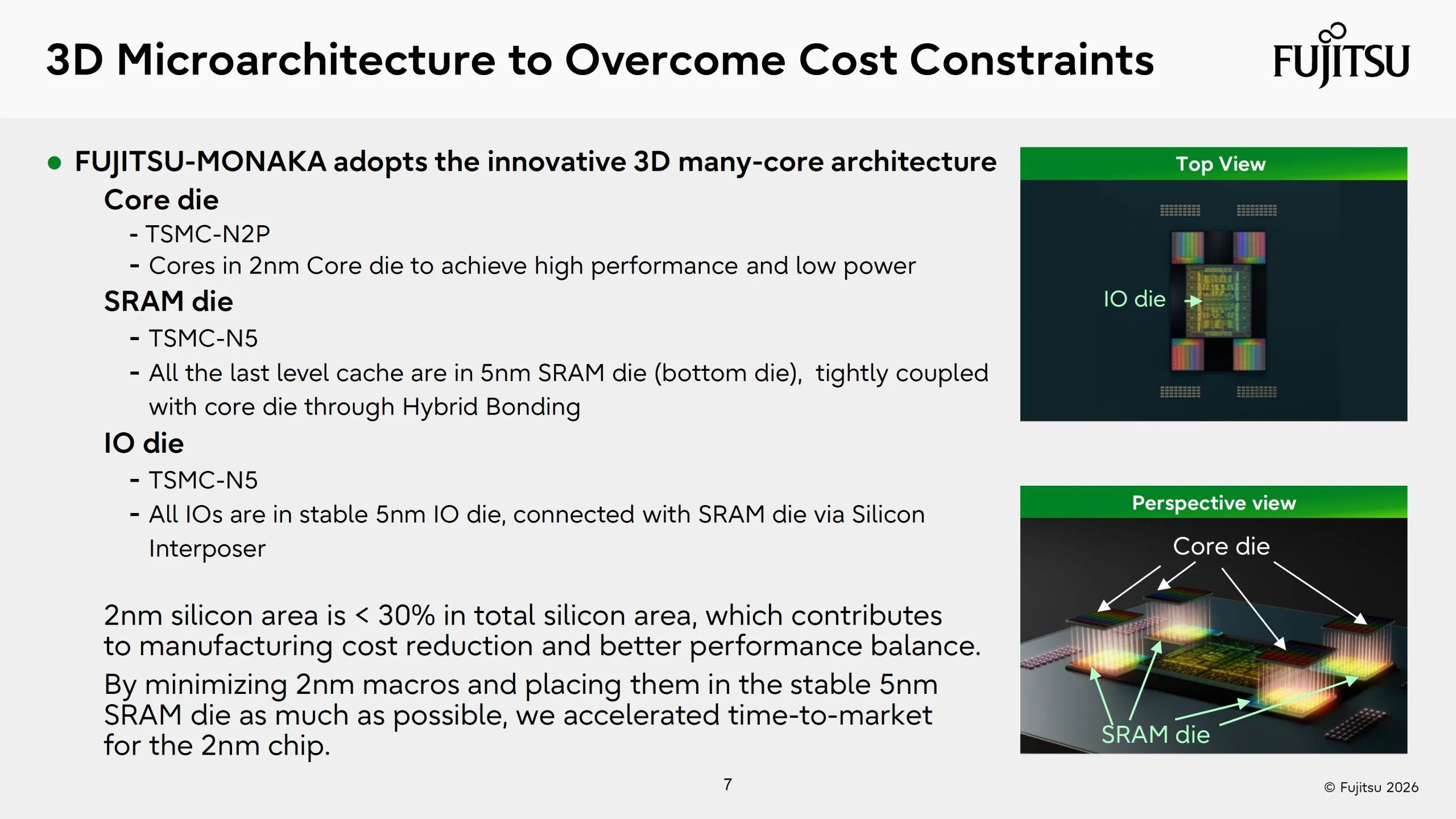
This "less than 30%" figure doesn't mean chip area was reduced by 30%. Rather, N2P is used for CPU cores, where transistor density and power efficiency translate directly into performance, while SRAM, I/O, and analog power circuits—which don't shrink as effectively with smaller process nodes—remain on N5. Fujitsu explained that by shifting these functions to N5, it can bring 2nm chips to market sooner while keeping manufacturing costs in check. However, the company has not disclosed defect density or post-stacking yield figures.
The base specification is 144 cores per socket, scaling to 288 cores per node in a two-socket configuration. Memory support includes 12 channels of DDR5 running above 8,000 MT/s, with external connectivity provided by 96 lanes of PCI Express 6.0/CXL 3.0. While narrowing the scope of the leading-edge process, Fujitsu expanded memory and I/O capacity to suit general-purpose servers.
What's Different About Moving the LLC to a Separate Die
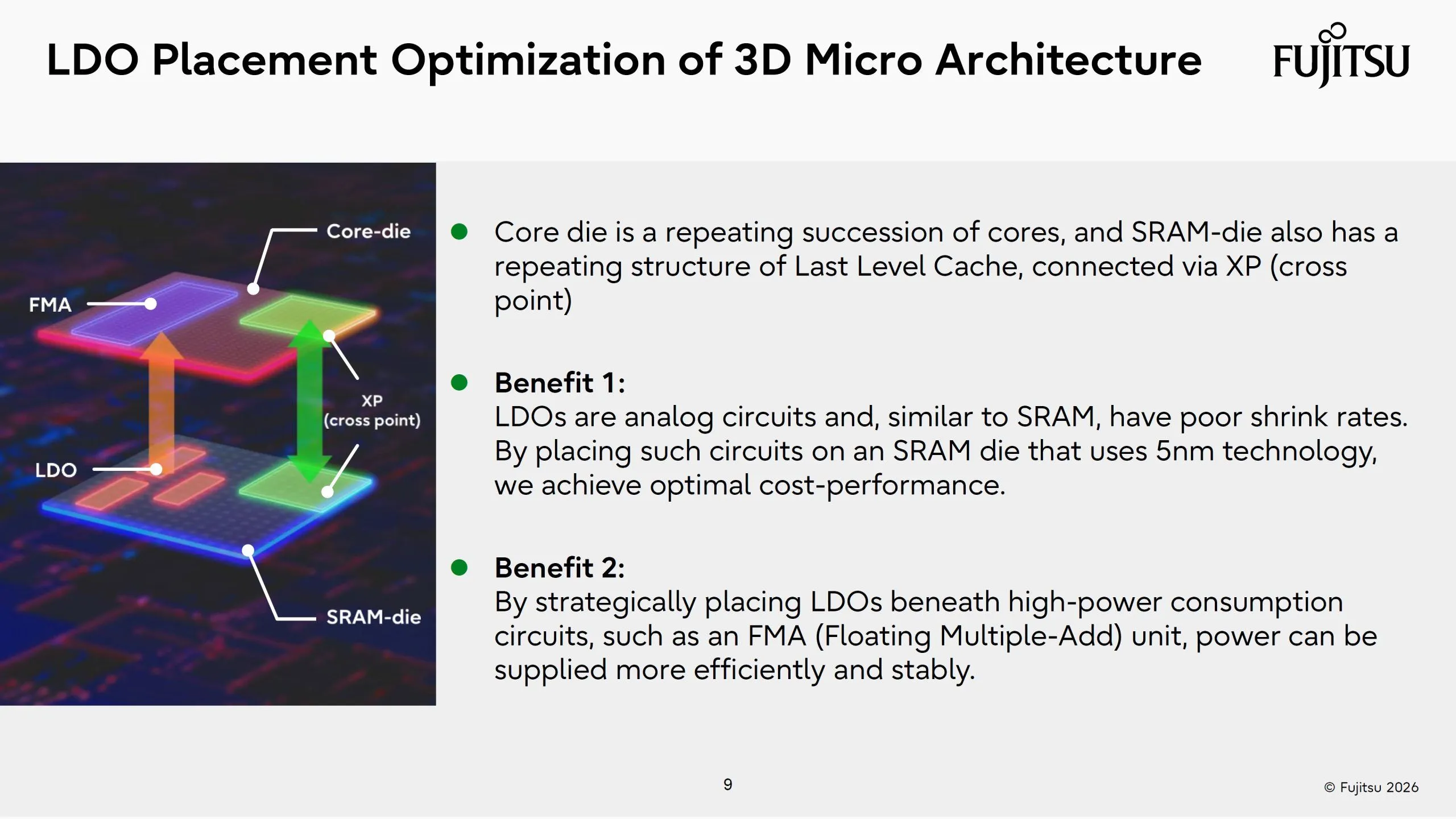
The entire LLC resides on the N5 SRAM die, connected to the N2P core die through a face-to-face (F2F) hybrid bond. Whereas AMD's 3D V-Cache stacks additional SRAM onto a compute die, MONAKA moves the entire LLC off the compute die altogether. The structure resembles Intel's Clearwater Forest, which stacks compute chiplets onto an active base tile handling cache and routing. However, MONAKA goes further by also relocating the LDOs used for per-core voltage control to the SRAM die.
Fujitsu addresses heat, signal latency, and power delivery through the vertical arrangement of components. The core die, which generates the most heat, sits at the top near the cooling surface, while the F2F bond minimizes the distance between the cores and LLC. Power flows from the package through a silicon interposer, then through TSVs and local LDOs within the SRAM die, before reaching the cores via the hybrid bond.
Placing the LDOs on N5 serves both cost and power-delivery purposes. LDOs are analog circuits that don't shrink well with process scaling, so Fujitsu positioned them on the SRAM die directly beneath power-hungry execution units such as the FMA. The goal is to deliver power through short, stable paths that support per-core DVFS control across all 144 cores.
Even so, vertical interconnects alone don't determine overall package latency. According to Tom's Hardware, Ian Cutress raised a question at Hot Chips about latency between distant core dies. Fujitsu pointed to the F2F bonding as the answer but did not disclose specific latency figures for cross-die communication. The actual paths and latencies between core dies and across NUMA domains will need to be verified once production units are available.
The distance visible to software can be configured according to workload needs. Options include a low-LLC-latency mode with eight NUMA nodes of 18 cores each, a balanced mode with four nodes of 36 cores each, or a high-memory-capacity mode treating all 144 cores as a single node. In the four-node configuration, each node has access to nearby L3 cache and three DDR5 channels. MPAM IDs for QoS control go up to 63 and are assigned independently of NUMA settings.
The Shift to 256-bit Isn't a Step Back from HPC
Fugaku's A64FX combined 48 compute cores with two 512-bit SVE units and 32 GiB of HBM2, achieving a theoretical memory bandwidth of 1,024 GB/s. MONAKA narrows this to two 256-bit SVE2 units per core while tripling the compute core count to 144. By replacing HBM2 with DDR5, Fujitsu has shifted the design's center of gravity from an HPC-specialized configuration toward a data center CPU offering flexible capacity and I/O options.
| Item | A64FX | FUJITSU-MONAKA |
|---|---|---|
| Instruction set | Armv8.2-A + SVE | Armv9.3-A + SVE2 |
| Compute cores | 48 | 144 |
| Vector units | 2× 512-bit SVE | 2× 256-bit SVE2 |
| Core-level cache | See product documentation | L1 instruction 64 KiB + L1 data 64 KiB, L2 512 KiB |
| Memory | 32 GiB HBM2, theoretical 1,024 GB/s | DDR5, 12 channels, over 8,000 MT/s |
| Process | 7nm | Core: N2P; SRAM/I/O: N5 |
| External I/O | PCIe Gen3, 16 lanes | PCIe 6.0/CXL 3.0, 96 lanes |
The move to 256-bit reflects Fujitsu's shift in target use case. In comments reported by Tom's Hardware during Q&A, Fujitsu's Ryohei Okazaki explained that the change was made to shrink core area and improve cost-performance for data center applications. Each core, measuring roughly 1.47 mm², packs two 256-bit load/store units, FP8 and INT8 matrix multiply support, a three-stage TAGE-based branch predictor, and six ALUs. It also includes ECC or duplication for L1/L2 caches, parity protection for execution units and registers, and hardware instruction retry for handling transient errors.
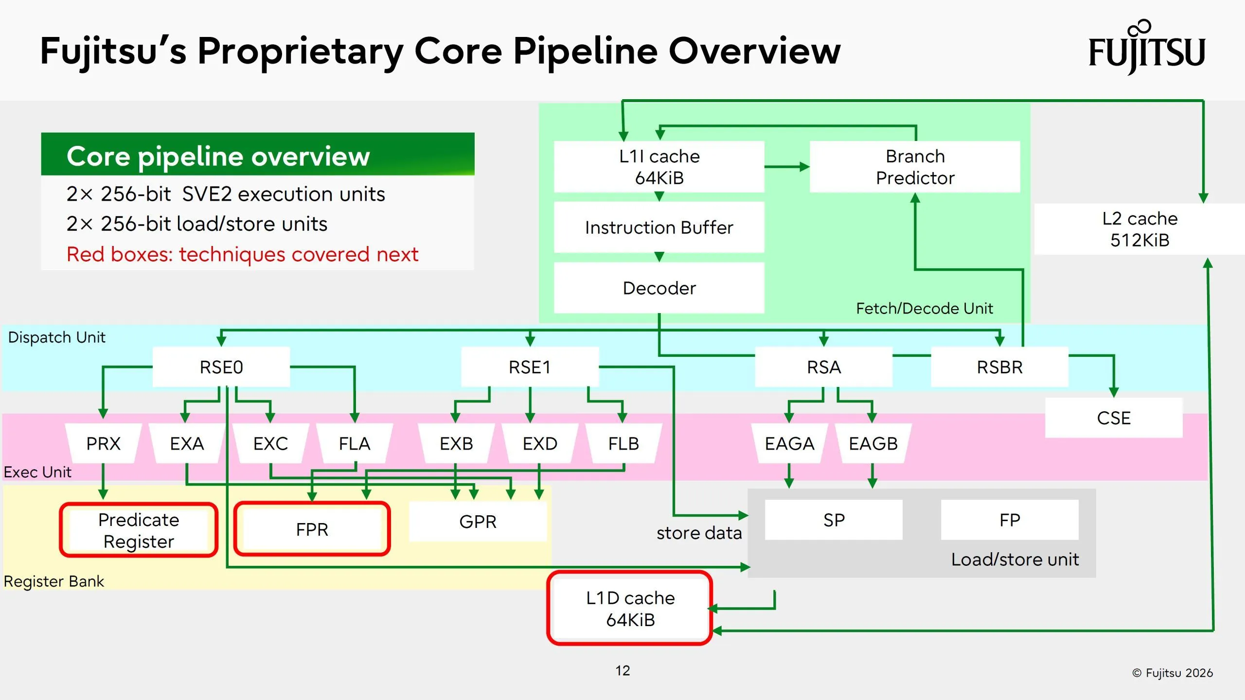
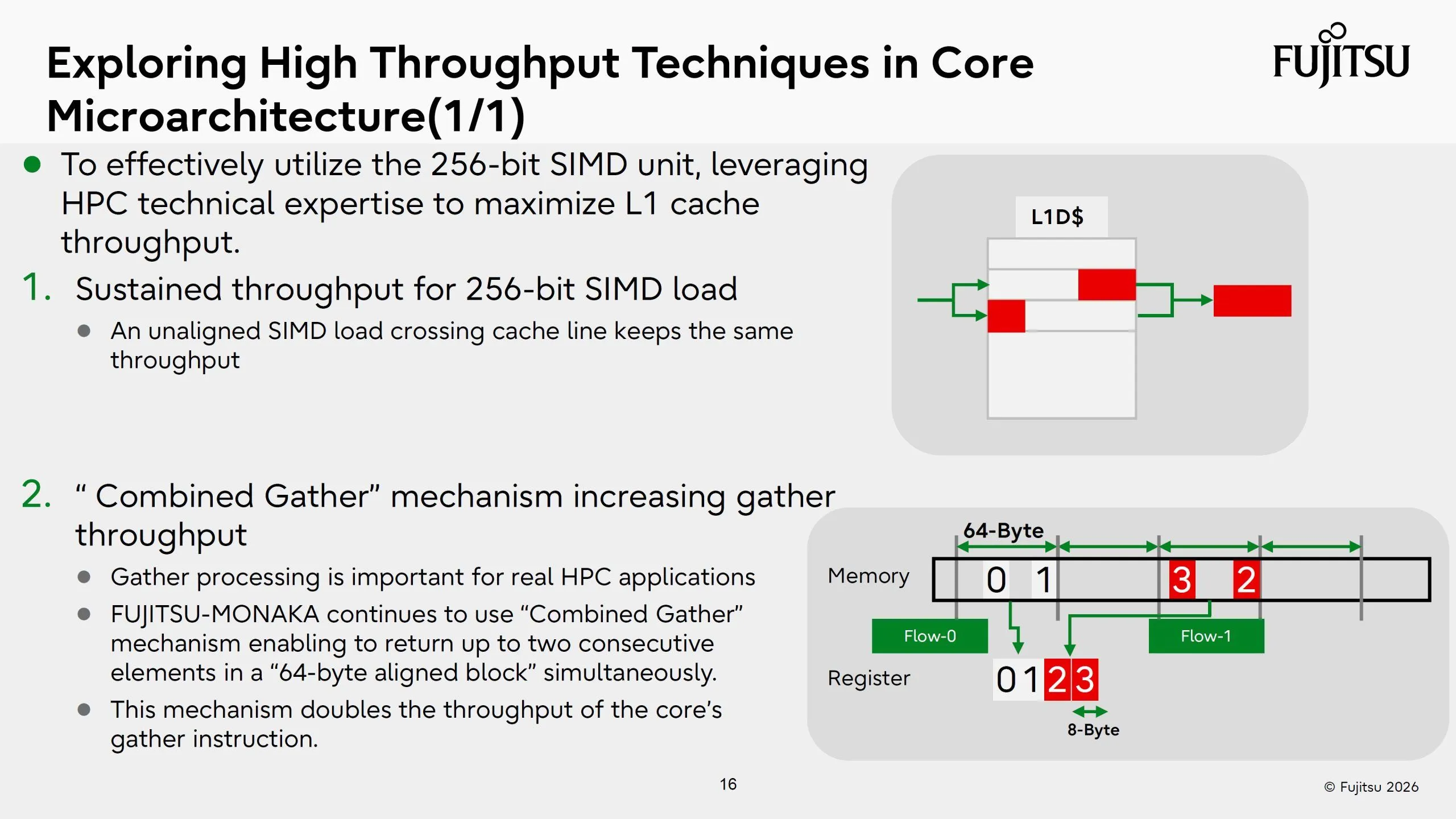
Several mechanisms help keep the narrower execution units fully utilized. The FPR cache avoids repeated accesses to the main FPR for operations like GEMM that reuse the same data repeatedly, reducing read power. Unaligned 256-bit SIMD loads maintain throughput even when they cross 64-byte cache line boundaries. Combined Gather can simultaneously return up to two contiguous elements within a 64-byte boundary, which Fujitsu says doubles Gather instruction throughput—though this is not a claim that overall application performance doubles.
Transfer widths from the core all the way to DDR5 are also aligned. The SVE2 pipeline and data fabric use two 32-byte-wide paths, while L1/L2/L3 cache lines and DDR5 bursts operate at 64 bytes. Rather than preserving 512-bit SVE, MONAKA's circuit design ensures that its two 256-bit paths avoid bottlenecks along the way.
Reading the Two SKUs: 350W and 500W
Fujitsu plans to offer two SKUs based on the same 144-core design: an air-cooled, high-efficiency version and a liquid-cooled, high-performance version. All performance figures presented at the talk are estimates, not measurements from production silicon.
| Item | High-Efficiency SKU | High-Performance SKU |
|---|---|---|
| TDP | 350W | 500W |
| Cooling | Air | Liquid |
| Base frequency | 2.1 GHz | 2.9 GHz |
| DGEMM | 4,355 GFLOPS (estimated) | 6,013 GFLOPS (estimated) |
| STREAM Triad | ~500 GB/s (estimated) | ~500 GB/s (estimated) |
| INT8 | 69.7 TOPS (estimated) | 96.2 TOPS (estimated) |
The 500W SKU has a TDP roughly 43% higher than the 350W SKU, while its estimated DGEMM and INT8 performance increase by about 38%. Simply dividing the stated performance figures by TDP suggests the high-efficiency SKU delivers about 3% better performance-per-watt. However, TDP is not the same as actual power draw, and Fujitsu hasn't fully disclosed the compiler settings, memory configuration, or precision conditions used in these estimated benchmarks. Based on the figures published so far, all that can be concluded is the general division of roles: the 350W SKU is designed for air-cooled deployments, while the 500W SKU pushes higher clock speeds under liquid cooling.
The 2029 MONAKA-X Belongs to a Different Generation
According to Fujitsu's roadmap, the 2027 MONAKA will be followed in 2029 by "FUJITSU-MONAKA-X," built on a 1.4nm process. MONAKA-X is planned to use Arm SME2 for AI workloads and serve as the CPU for Fugaku NEXT, paired with NVIDIA GPUs. For CPU-GPU connectivity, Fujitsu is evaluating high-bandwidth, cache-coherent NVLink-C2C/NVLink Fusion as a strong candidate.
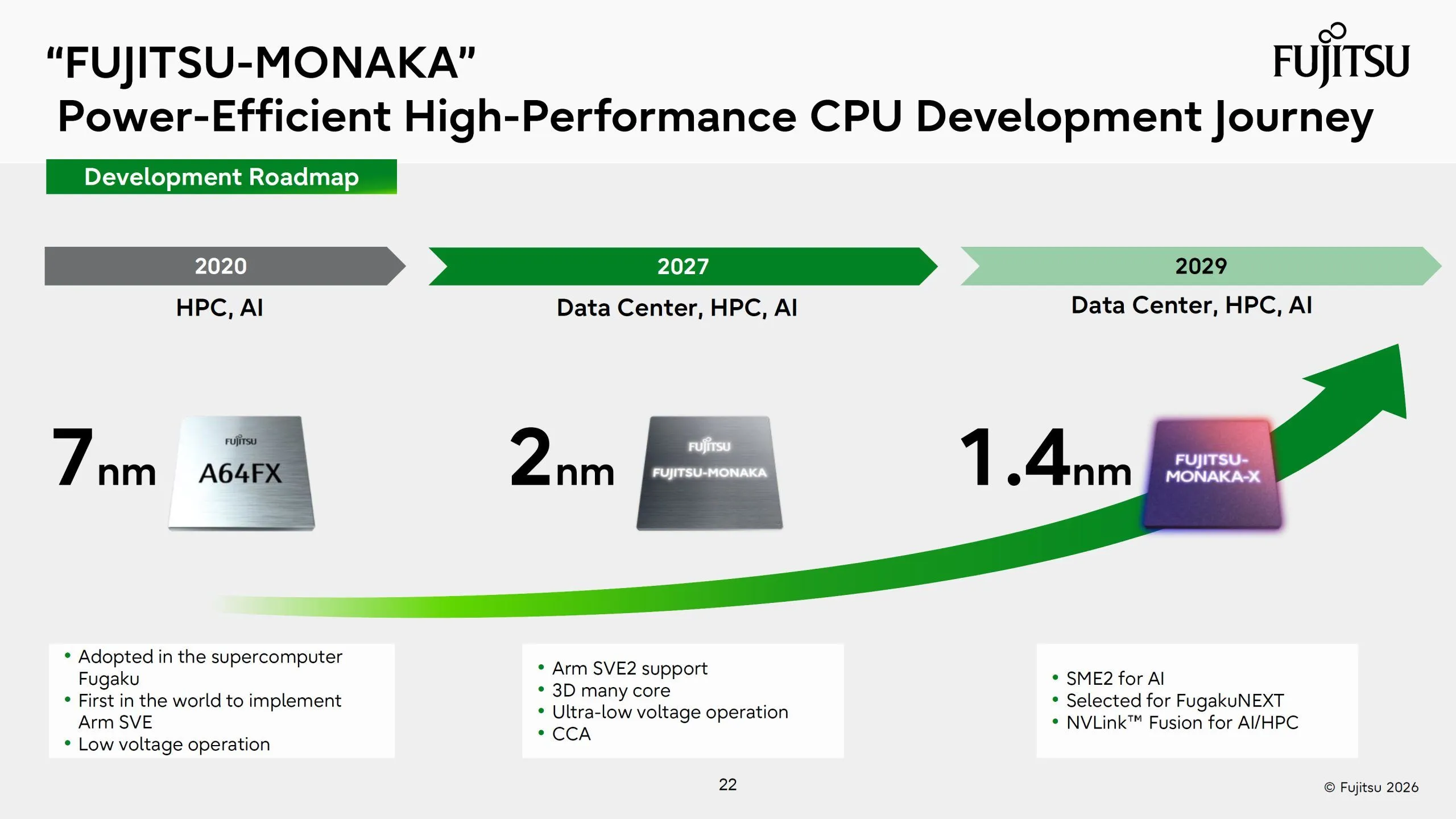
These timelines should not be conflated. MONAKA, slated for product shipment in 2027, is a general-purpose data center CPU equipped with DDR5 and PCIe/CXL support. MONAKA-X, by contrast, is a successor plan intended to power Fugaku NEXT around 2030, and details such as the 1.4nm foundry partner, core count, and final GPU interconnect specification have not been officially confirmed.
A proper assessment of MONAKA will only be possible once LLC capacity and maximum memory capacity are clarified, and once NUMA-to-NUMA latency, actual power consumption, and real-world application performance have been measured. If Fujitsu can reproduce these estimated figures in practice, it will be able to bring the HPC expertise it built with A64FX into the broader Arm server market, spanning enterprise and cloud customers. The 1.4nm process, SME2 support, and NVLink Fusion connectivity planned for MONAKA-X remain separate matters that will need to await finalized detailed designs, independent of how MONAKA itself performs.