

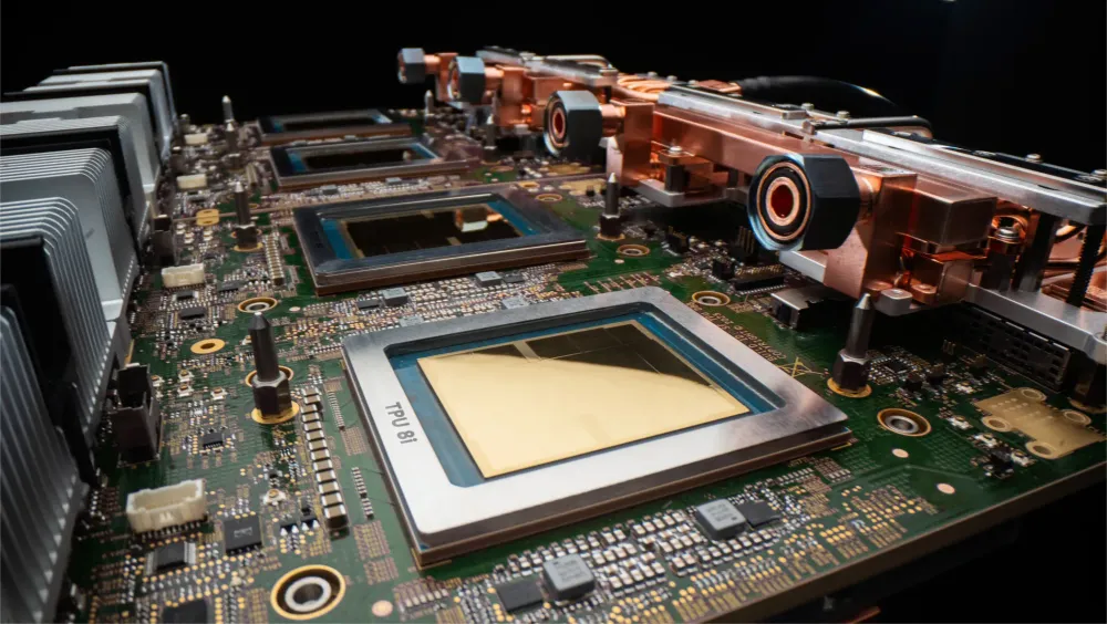
Fubon Research has presented an estimate that Google plans to secure 12 million to 15 million 9th-generation TPUs in 2028. The upper figure exceeds the company's own projection for NVIDIA's data center AI GPU shipments in the same year. However, Google has only officially disclosed information up to its 8th generation, and neither this quantity nor the specifications of the 9th generation have been officially announced. What's emerging is a shift in which Google is expanding TPUs from computing infrastructure for its own services to system sales aimed at customers. The view that the company is moving to secure manufacturing and packaging capacity from multiple partners is based on Fubon's estimate and reporting from The Information.
The Maximum of 15 Million Is Not an Official Google Target
According to an excerpt from a research note Fubon published on July 30, Google plans to "have" 12 million to 15 million TPUs in 2028. The note also suggests that the 9th-generation part will consist of 4 compute dies, and that the production capacity consumed in 2028 will more than double that of 2027. The range spans 3 million units, and Fubon itself states that it does not have detailed knowledge of the allocation between TSMC and Intel.
Here, "have" does not mean that the entire volume will be newly produced and sold externally within 2028. The figure could be a mix of TPUs used in Google's own data centers, those provided to customers via Google Cloud, and TPU systems delivered to customer facilities. The 12 million to 15 million figure should be read as an analyst's estimate of a plan, not a confirmed order or actual shipment volume.
The latest products Google announced in April are the 8th-generation training-focused "TPU 8t" and inference-focused "TPU 8i," with general availability planned for the second half of 2026. The company has explained that it begins designing TPUs several years in advance, so it wouldn't be unusual if supply planning for 2028 were already underway. That said, Google has not disclosed the name "9th generation," its launch timing, the 4-die configuration, or the quantity.
The Blind Spot in Comparing 15 Million TPUs to 12.4 Million GPUs
Fubon estimates that NVIDIA's data center AI GPU shipments will grow from 8.2 million units in 2026 to 12.4 million units in 2028. Google's upper bound of 15 million exceeds this figure, but the two "units" cannot be measured on the same yardstick.
Even looking only at Google's 8th generation, the 8t and 8i serve different roles. The 8t's Superpod bundles 9,600 chips, featuring a shared HBM of 2PB and 121 ExaFLOPS of compute performance. The 8i, on the other hand, is designed with 288GB of HBM per chip and 19.2Tb/s of inter-chip connectivity, aimed at cost-efficient inference. Given differences in generation and use case, plus memory capacity and network configuration, one cannot directly compare training capability or inference throughput based on unit counts alone.
The sales models also differ. NVIDIA's figure is an estimate of commercial GPU shipments, whereas Google's figure appears to represent a holdings plan combining internal use, cloud provisioning, and system sales. Alphabet began recognizing revenue from a limited TPU system supply agreement in Q2 2026. The counterparties are customers who need on-premises infrastructure for specialized, large-scale workloads, or who provide such infrastructure. Most of the revenue is expected to be recognized in 2027. Therefore, even if the 15 million figure is realized, it does not necessarily translate into external sales revenue or market share on the same scale as NVIDIA.
Still, the strategic implications are significant. If Google can cover a substantial portion of AI demand with its own chip designs, it won't have to rely solely on external GPU supply to expand compute capacity. What matters more than ranking by unit count is how much operating capacity Google can supply to both its own services and external customers.
Fubon's Estimated 4-Die Configuration and the Roles of TSMC and Intel
If the 9th generation indeed adopts a 4-compute-die configuration as Fubon suggests, supply capacity will not be determined by logic wafer count alone. Packing 4 good dies together with HBM into a single package requires advanced packaging processes, including substrates, interconnect technology, and testing. Die dimensions, manufacturing process, and yield remain unknown, making it impossible to back-calculate required capacity from quantity figures.
TSMC has raised its 2026 capital expenditure to $60 billion to $64 billion, allocating 10% to 20% of that toward advanced packaging, testing, masks, and related areas. In Taiwan, the company plans to build 13 fabs for advanced processes and advanced packaging over the coming years. While TSMC states it doesn't foresee bottlenecks in its capacity expansion plans, it has also noted that developing advanced technology through to mass production ramp-up takes more than five years. This is not a guarantee that allocation for Google will be sufficient.
Regarding Intel, The Information reported in June, citing sources, that Google placed an order for more than 3 million TPUs for 2028 after testing Intel's advanced packaging technology over several months. Neither Google nor Intel has confirmed this. Intel's EMIB is a 2.5D technology that uses small embedded silicon bridges within the package substrate to connect logic dies to each other or to HBM, and it has a track record of mass production using external companies' silicon.
However, the report on the Intel order does not confirm that TPU logic front-end manufacturing is shifting away from TSMC entirely. The specific division of labor across wafer fabrication, advanced packaging, and testing remains undisclosed. What's realistic for Google is not choosing between TSMC or Intel exclusively, but rather diversifying suppliers at each process stage to build a structure where a bottleneck at any single point doesn't halt the entire pipeline.
Demand Is Visible; Power and Implementation Remain the Constraints
Evidence supporting large-scale demand already exists. In October 2025, Anthropic announced access to up to 1 million TPUs, with plans for capacity well exceeding 1GW to come online during 2026. In April 2026, the company revealed a contract with Google and Broadcom for multi-gigawatt-scale next-generation TPU capacity, to be brought online starting in 2027. While this figure doesn't map one-to-one with chip count and power consumption, it demonstrates that Google carries substantial demand beyond its own models.
Alphabet's capital expenditure in Q2 2026 reached $44.9 billion, totaling $80.6 billion for the first half of the year. The primary use is technology infrastructure including servers and data centers, not TPU spending alone. In announcing its 8th-generation TPU, Google itself explained that power, just as much as chip supply, is a constraint in data centers, and it is combining this with 4th-generation liquid cooling equipment.
Clues for verifying the 15 million figure for 2028 will emerge in stages: first, the general availability of the 8t and 8i in the second half of 2026; next, the ramp-up of TPU system sales revenue and Anthropic-directed capacity in 2027; and finally, official disclosures regarding the 9th generation and the division of responsibilities with Intel. Even with a large volume of chips prepared, unless HBM, packaging, cooling, power, and data centers all align on the same timeline, it won't translate into operational capacity. What Fubon's estimate really questions is not so much the unit-count race against NVIDIA, but whether Google can bring this entire supply chain together by 2028.