

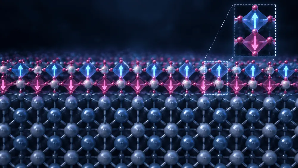
A research team including the University of Nebraska–Lincoln has shown experimentally that hafnium oxide-based materials, widely used in semiconductors, can exhibit antiferroelectricity that arises from the crystal itself. In single-crystal thin films of 10% La-doped hafnia under compressive strain, the ordering in which neighboring electric dipoles point in opposite directions persisted down to a thickness of 0.6nm, equivalent to one unit cell.
The results were published in Science on September 24, 2026. The transition temperature of 850±50°C that the authors determined is also remarkably high, but it does not mean that a finished energy-storage device operated at 850°C.
The key point of this work is that it offers strong evidence, from both crystal structure and electrical response, on the long-running debate over whether hafnia-based materials are truly antiferroelectric.
Confirming "intrinsic" antiferroelectricity in La-doped hafnia
In an antiferroelectric, the electric dipoles produced by small atomic displacements line up in opposite directions in neighboring regions. The net polarization seen from outside therefore nearly cancels out, but when a sufficiently strong electric field is applied, the dipoles align in the same direction and a large polarization appears. When the field is removed, the material returns to the low-polarization state.
Because this switching can be used to store electrical energy temporarily and release it quickly, the materials are expected to find applications in high-density capacitors, solid-state cooling and memory.
However, even when the double hysteresis characteristic of antiferroelectrics was observed in hafnia, it was not conclusive proof of antiferroelectricity.
Polycrystalline thin films readily contain a mixture of crystal phases and defects, and similar hysteresis shapes can arise from defects that pin polarization, from "wake-up," in which polarization grows with repeated field cycling, or from a phase transition from a tetragonal phase to a ferroelectric orthorhombic phase.
The subject of the authors' publicly available manuscript was a single-crystal thin film of Hf0.9La0.1O2 (LHO) grown on a (111)-oriented yttria-stabilized zirconia (YSZ) substrate.
The results therefore cannot be applied directly to undoped HfO2 in general.
Adding 10% of La, which has a large ionic radius, expands the LHO lattice. Meanwhile, the YSZ substrate strongly compresses the film in the in-plane direction. The team explains that this epitaxial compressive strain stabilizes an antipolar orthorhombic phase in which neighboring dipoles are arranged in opposite directions.
Confirmed at the atomic arrangement, not just by double hysteresis
The team combined several measurement techniques to confirm the existence of the antipolar orthorhombic phase.
First, X-ray diffraction captured the lattice distortion characteristic of the orthorhombic phase, and the team produced films free of the monoclinic phase up to at least 30nm.
X-rays, however, have difficulty resolving the positions of relatively light oxygen atoms. The team therefore examined a 30nm-thick film with neutron diffraction and observed half-integer peaks indicating that the unit cell has double periodicity along the crystal's b-axis.
This is consistent with a structure in which the direction of oxygen displacement reverses between adjacent polar layers.
The team also directly observed the arrangement of oxygen atoms using annular bright-field scanning transmission electron microscopy.
In the images, polar stripes were lined up with nonpolar layers between them, and in neighboring stripes the oxygen displacements pointed mainly in opposite directions. Some layers pointed in the same direction, which the team interprets as antiphase boundaries where antipolar domains meet.
This confirms a structure in which dipoles alternate in direction not only in the average crystal structure but also at the atomic scale.
The electrical response was measured on a separately prepared 2.2nm-thick film.
When a bipolar triangular wave was applied across a 3.5µm electrode gap of comb-shaped Pt electrodes formed on the surface, a characteristic double hysteresis appeared, moving back and forth between the antipolar and polarized states.
Even after 5,000 cycles at 20Hz, the hysteresis loop showed no noticeable change.
If defect-induced polarization pinning were the main cause, repeated field cycling could change the loop toward one resembling a ferroelectric. The results differed from that behavior.
The absolute polarization values, however, should be treated with caution.
The team estimated the effective area semi-quantitatively from the number and length of the comb electrode fingers and the film thickness.
The team also explains that the increase in remanent polarization at higher frequencies results from a metastable state: after the material moves from the antipolar phase to the polarized phase, a high energy barrier prevents it from returning immediately to its original state.
This is an interpretation combining experimental results with DFT calculations, not a mechanism determined solely from direct observation of the atomic structure.
Antipolar order did not disappear even at 0.6nm
It is generally thought that antiferroelectric order weakens as films get thinner and disappears below a certain thickness.
In the LHO/YSZ films, however, the opposite trend appeared.
Using reflection high-energy electron diffraction, the team examined the intensity ratio between a diffraction peak that appears only in the orthorhombic phase and one that appears in both the orthorhombic and tetragonal phases, as an indicator of antipolar order.
This ratio increased as the film was thinned from 10nm, and changed sharply between 0.6nm and 0.5nm.
0.6nm corresponds to roughly one unit cell, while 0.5nm is below that. In other words, antipolar order was maintained down to the extreme thinness of a single unit cell.
No structure that significantly disturbed the antipolar order was seen at the interface with the substrate, either.
Scanning transmission electron microscopy showed that the lattice strain in LHO reached nearly its final value within the first unit cell from the interface, and that the strain also extended into the top two atomic layers on the YSZ side.
In addition, a DFT model with five atomic layers of HfO2 placed on a ZrO2 substrate maintained a lattice distortion close to that of bulk orthorhombic material right up to the interface.
In this system, then, the interface with the substrate appears not to destroy the antipolar order but to contribute to stabilizing the orthorhombic phase through compressive strain.
Comparison with other compositions also reveals the effect of La doping.
On the same YSZ(111) substrate, undoped HfO2 and Hf0.5Zr0.5O2 showed orthorhombic order that weakened sharply once the film thickness fell to about 1–2nm.
LHO, on the other hand, has a larger lattice constant because of the La, so it receives stronger compressive strain from the YSZ substrate.
The authors explain that as the film gets thinner, the influence of this strain grows stronger, making the antipolar orthorhombic phase energetically stable.
The 0.6nm result therefore cannot be separated from the conditions under which it was obtained: single-crystal LHO with 10% La grown on a YSZ(111) substrate.
What "850°C" and "0.6nm" mean
The figure of 850±50°C does not mean a thin-film device was operated 5,000 times at that temperature.
The team measured the diffraction peak intensity ratio while varying the temperature, and determined the transition temperature at which the antipolar orthorhombic order is lost and the film shifts to the high-temperature tetragonal phase.
For a film about 10nm thick this temperature was about 600°C, but when the film was thinned to the 0.6nm level it rose to 850±50°C.
The temperature at which order is lost normally tends to fall as films get thinner, but in this LHO it rose instead. That is the important meaning of the 850°C figure.
In version 2 of the authors' arXiv manuscript, 850±50°C is given as the transition temperature of the orthorhombic order in 0.6nm-level LHO films.
The electrical cycling stability that was confirmed, meanwhile, covers only a 2.2nm-thick film measured for 5,000 cycles at 20Hz.
The paper and the university's announcement do not report energy density, charge-discharge efficiency, power density, device operation at 850°C, or manufacturable capacitors.
The existence of an antiferroelectric phase and how much electrical energy an actual device can store are separate evaluation items.
The same applies to the 0.6nm figure.
The main text of the paper shows by diffraction that antipolar structural order is maintained down to this thickness, and the supplementary materials say double hysteresis was also confirmed.
However, the 5,000-cycle result obtained on the 2.2nm film cannot be treated as the durability of a 0.6nm film.
The 5,000-cycle test is meaningful for verifying that the observed hysteresis does not originate from defects, but it is not a cycle count that supports the lifetime of a practical product.
Applications in energy storage, cooling and memory are still ahead
The significance of this result lies not in setting a record for energy storage performance but in clearly showing that antiferroelectricity can be engineered in hafnia-based materials.
If the antipolar orthorhombic phase exists as a stable state intrinsic to the crystal and can be switched to a polarized phase by an electric field, research can move toward designing antiferroelectricity by controlling composition, strain and interface structure, rather than relying on defects by chance.
Unlike many representative antiferroelectrics, hafnia-based materials also contain no lead. Hafnium oxide is already widely used in semiconductor manufacturing, and the possibility that it functions even as an ultrathin film is attractive for small capacitors and memory devices.
However, the term "CMOS-compatible" should not be taken to mean that the films made here can be introduced as-is into current mass-production semiconductor lines.
In this experiment, single-crystal LHO films were grown on single-crystal YSZ substrates by pulsed laser deposition.
Whether the same antipolar phase can be formed reliably in the polycrystalline films common in volume manufacturing, or with different electrodes and substrates, and whether film thickness and properties can be reproduced uniformly over large areas, are challenges for the future.
To assess practicality, it will be necessary to measure energy density and energy recovery efficiency, including up to the dielectric breakdown field, on the same samples, and to examine whether they withstand long-term electric-field cycling and thermal cycling.
For solid-state cooling, the temperature change obtainable when the electric field is varied must be measured. For use as memory, read/write speed and data retention time must also be evaluated.
If such performance can be reproduced in structures close to mass production, hafnia could expand beyond its role as a gate insulating material to take on functions such as electrical energy storage, thermal control and information storage.