

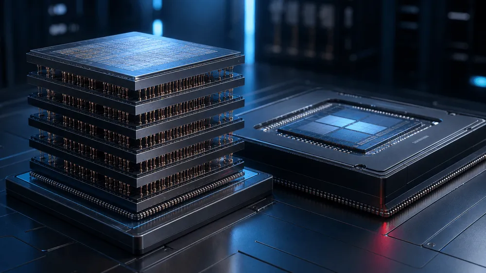
On August 3, 2026, Sandisk and SK hynix published the first technical specification for High Bandwidth Flash (HBF) through the Open Compute Project (OCP). The standardization effort, which began in February, advanced over roughly six months into a common set of design criteria covering host connections, electrical specifications, packaging, and software operations. HBF is a concept that stacks NAND flash to place larger capacities than HBM near AI accelerators. What has come together now is not the product itself, but the shared specification for connecting memory to accelerators.
Connections and Implementation Standardized in About Six Months
The initial specification defines the system interface along with electrical and technical guidelines, as well as baseline performance expectations. Its scope includes the host interface linking xPUs and HBF, the reliability and packaging of HBF die stacks, and software guidance for reading and writing. It also covers how HBF should be handled from CPUs, GPUs, and dedicated accelerators.
Google and Tenstorrent joined the consortium partway through the standardization process, participating in technical validation and specification development. While Sandisk and SK hynix served as the primary contributors, both companies that operate AI infrastructure and those that design accelerators also joined the validation work. Although the announcement from the two companies does not detail the specific contributions made by Google and Tenstorrent, the participant base expanded from the two memory makers to include system-side players.
The specification was made public to the industry through the OCP framework. At the same time, OCP places HBF within the Storage domain's Semi-Private Workstream, and has established defined procedures for joining collaborative development or providing feedback. Viewing the finalized specification and participating in drafting the next version are separate matters.
A Supplementary Layer Bridging HBM and SSDs
SK hynix describes HBF as a new memory tier that adds a layer between HBM and SSDs. HBM handles workloads that require the highest bandwidth, while HBF keeps larger model weights closer to the compute engine. The goal is to reduce how often weights must be transferred from SSDs, while avoiding a configuration where HBM alone must cover the entire capacity. The two are not meant to replace each other but to be used together within the same system.
At the core of HBF is Sandisk's CBA (CMOS directly Bonded to Array) technology, which directly bonds NAND memory cells to CMOS circuitry, combined with 16-layer die stacking. NAND retains data even when power is cut and does not require the refresh power that DRAM does. Sandisk aims to leverage this characteristic for storing model weights that are not frequently rewritten.
However, Sandisk acknowledges that HBF has longer latency and larger page sizes than HBM. The company's own performance comparisons were also targeted at use cases involving reading pretrained weights during inference. The OCP specification includes read/write guidance and reliability guidelines, and Sandisk is designing product-level technologies to address durability and high-temperature operation.
1.6TB/s and 512GB Are Not OCP-Mandated Values
The first-generation HBF targets that Sandisk presented in July 2025 were a read bandwidth of 1.6TB/s, 256Gb per die, and a total capacity of 512GB across a 16-die stack. The company has also cited a footprint, power consumption, and stack height comparable to HBM4. However, these are development targets for Sandisk's own product and are not figures that the current OCP specification guarantees across all implementations.
The basis for these performance claims also comes with caveats. Sandisk states that in an internal simulation reading 8-bit pretrained weights from the Llama 3.1 405B model, the performance gap between HBF and a hypothetical HBM with unlimited capacity was within 2.2%. This comparison reflects results on a model running one kernel at a time, not measurements of mixed workloads or write performance on actual hardware. Whether the system can stably deliver 512GB of capacity and 1.6TB/s of bandwidth simultaneously remains something to be confirmed with real products.
This distinction is essential for gauging how far standardization has actually progressed. The current announcement does not include a specification version number, conformance testing procedures, or certification scheme details, nor does it disclose detailed numerical requirements. Even with a common interface defined, it is not guaranteed that HBF and accelerators from different vendors will be interchangeable.
Measuring Interoperability After Samples Ship
As of August 2025, Sandisk had indicated targets of shipping initial samples of HBF memory in the second half of 2026, and initial samples of inference devices incorporating HBF in early 2027. The publication of the specification represents preparation for moving from a phase where those samples are evaluated as standalone memory to a phase where they are tested as part of a system that includes hosts and software. SK hynix has projected that demand for composite memory including HBF will grow around 2030, meaning the standard has been put in place ahead of the market's actual takeoff.
On real hardware, it will be necessary to verify connections with different hosts, power consumption during sustained reads, reliability under high temperatures, and NAND durability. Furthermore, unless software can properly control what data is placed on HBM versus HBF, increasing capacity alone will not shorten response times. Since pricing has not been disclosed, reductions in total cost of ownership will also need to be measured configuration by configuration.
The participation of Google and Tenstorrent marks an entry point for beginning this kind of system-level validation. If connections aligned with the specification are reproduced in the samples expected in the second half of 2026, and if the division of roles with HBM functions properly in the inference devices expected in early 2027, HBF can advance from being a new NAND product to becoming part of the AI memory hierarchy. What will determine success after the specification's publication is not the 512GB capacity figure itself, but whether that capacity can be used consistently across computing infrastructure from multiple companies.