

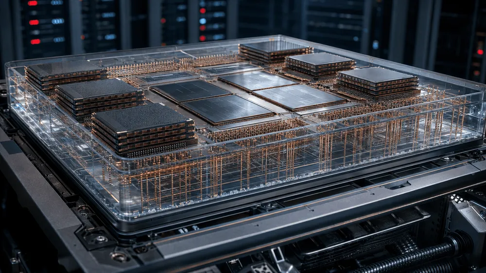
ETNews reported on July 27 that Huawei has drawn up a roadmap to mass-produce semiconductor glass substrates in 2027 using China's supply chain. According to the report, partner manufacturers will begin production in line with Huawei's requirements and apply the substrates to advanced chips such as the Ascend AI accelerator.
The timing overlaps with the fourth quarter of 2027, when Huawei is set to launch Ascend 960. However, Huawei's publicly disclosed chip roadmap makes no mention of glass substrates, and adoption for Ascend 960 has not been confirmed. What has emerged is not a product specification, but a move to consolidate even the back-end processes—which turn AI chips into functioning large-scale systems—among Chinese companies.
A 2027 Roadmap Tying Together BOE and Three Other Companies
ETNews named four companies as manufacturing partners: BOE, Visionox, Yuntian Semiconductor, and AKM Meadville. While Huawei and its partners are building a materials and equipment supply chain within China, they are reportedly also approaching South Korean materials, components, and equipment companies for cooperation. AKM Meadville has officially announced that it will give a presentation on glass-core ABF substrates at the TGV Technology Forum in 2025, which at least confirms that candidate companies are indeed pursuing glass substrate technology.
According to another ETNews article, Chinese companies are already at the prototyping stage, and once they pass the performance evaluations Huawei requires, they intend to switch to mass production. The report also cited industry assessments that Chinese firms' TGV (Through Glass Via) formation capability is not far behind that of South Korean companies. On the other hand, challenges remain in plating—stably coating the holes formed in the glass with metal—and in controlling the micro-cracks that occur during processing.
In other words, 2027 is not a release date for an announced finished product. According to ETNews, it is the target year for beginning production after aligning samples made on pilot lines with Huawei's required specifications and passing performance evaluation and mass-production qualification. Huawei has not announced this plan, and neither the investment amount nor any mass-production contract has been confirmed.
A "Multi-Die Integration" Timeline Overlapping with Ascend 960
Under Huawei's official plan, Ascend 950DT is slated for the fourth quarter of 2026, Ascend 960 for the fourth quarter of 2027, and Ascend 970 for the fourth quarter of 2028. The policy is to release a new series roughly every year, doubling computing performance each time.
The structure of Ascend 950 illustrates well how important back-end processes are. Huawei combines the same Ascend 950 die with proprietary HBM tailored to different use cases and packages them separately. Ascend 950DT, aimed at training and decoding, is planned to carry HiZQ 2.0 offering 144GB and 4TB/s, with inter-chip connection bandwidth reaching 2TB/s. With Ascend 960, both computing and memory performance are set to double compared to the 950, and the number of connection ports will also double.
With this kind of scaling, making the logic die alone faster will not raise system performance. Power must be delivered to the die and HBM, high-speed signals must be routed over short distances, and the mounting area must be expanded while suppressing package warpage. If the 2027 glass substrate plan is accurate, it makes sense for the timeline to align with the Ascend 960 generation. However, no product name or substrate structure linking the two has yet been disclosed.
Rather than emphasizing individual chips, Huawei is putting SuperPoD—which connects NPUs at massive scale—front and center. The actual Atlas 950 SuperPoD unit unveiled on July 17 is configured with 1,024 cards, delivering 1 EFLOPS in FP8, 2 EFLOPS in FP4, and a unified memory space of 256TB. At its global unveiling in March, the same system was described as scalable up to 8,192 NPUs. What glass substrates would handle is not this inter-rack connectivity, but the density and stability inside the package that houses each NPU and its memory.
Glass Substrates Are Not a Substitute for EUV Lithography
What glass substrates improve is the semiconductor package, not the front-end process of patterning circuits on the silicon die. Organic substrates become more prone to warping from heat and manufacturing processes as packages grow larger, making it difficult to precisely stack fine wiring. Glass, by contrast, offers better flatness and dimensional stability, allowing TGVs to be arranged at high density and enabling logic chips and HBM to be connected over a larger area.
Intel has stated that its own glass substrate technology can reduce pattern distortion by 50% and potentially increase connection density by up to 10 times compared to organic substrates. It also cited large packages for AI, data centers, and graphics as initial use cases. These figures represent Intel's technical outlook and are not measurements from products by Huawei or BOE.
Therefore, introducing glass substrates does not resolve the shortage of EUV lithography equipment. Nor is it a technology for shrinking the Ascend logic die within the same area. What it can achieve is bundling multiple dies and memory—made with whatever process is available—at high density, and improving power delivery and signal quality. It can serve as a means of compensating for front-end process constraints through back-end system design, but it is not a replacement.
From a 1,000-Sheet-per-Month Pilot Line to Mass-Production Yield
BOE, named as a candidate for Huawei's plan, has disclosed its preparatory stages in considerable detail in company materials. The company began technical research in 2020, and in 2022 invested 390 million yuan to set up wafer-level experimental equipment. In 2024, it expanded the scale with a 993 million yuan investment in a panel-level pilot line, completing the installation and calibration of major equipment in 2025. Huawei's requirements could potentially link this five-plus-year investment to mass-production qualification for a specific product.
In the first half of 2026, BOE ran fully automated equipment through the line. Its design capacity is 1,000 sheets per month, and it has been sending 20-layer large samples to customers, some of which have moved on to technical trials following proof of concept.
However, 1,000 sheets per month is the pilot line's design capacity, not the number of good units shipped. BOE explicitly states that it has not yet reached mass-production yield, nor has mass-production revenue begun. If Huawei's requirements are added to the mix, BOE's customer trials—whose specific applications and customer names were not disclosed in company materials—could lead to qualification work for AI accelerators. This is where the biggest change from the report lies.
Compared with other countries' plans, it is difficult to say that Huawei's "one-year lead" is confirmed. Samsung Electro-Mechanics is making prototypes on a pilot line in Sejong, and officially plans mass production from 2027 onward through a joint venture. DNP launched a pilot line for TGV glass-core substrates in December 2025, began providing samples from early 2026, and aims to start mass production in fiscal 2028. Each company's roadmap differs in terms of which stage—from prototyping to customer adoption—it refers to.
It Becomes a Strategy Only Once Product Names and Yield Numbers Emerge
Huawei's AI strategy is moving toward combining Ascend dies with proprietary HBM and connecting them to SuperPoD via UnifiedBus. Glass substrates could become a candidate for supporting larger packages and higher-density wiring within that framework. But at this point, what has been publicly disclosed is the product plan on the Ascend side, while the glass substrate side remains a reported mass-production target.
The next things to watch are more concrete than a date: Will Huawei reveal product names such as Ascend 960 along with the substrate structure? Will BOE and others disclose actual yield and good-unit counts rather than just pilot-line throughput? And will they pass reliability evaluations for TGV, plating, and micro-cracks, and move on to mass-production contracts and revenue? If all three come together in 2027, glass substrates will move from being a Chinese research topic to becoming part of Huawei's AI chip supply chain.